
Over the last two weeks an enormous amount of progress has been made. First, after having successfully solved the dead gate driver issues, we then had a MOSFET die. The cause was identified as V_GS going out of range. This was resolved through a two-part solution. First, the output line of the gate driver was given two clamp diodes, one to VDD and one from GND. This effectively limited the output voltage of the gate driver from -0.3 – 12.3V, well within the MOSFET’s operating range. Second, the MOSFET source is connected to the ground terminal of the 48V power supply, which was not directly tied to the control circuit grounds. This was initially viewed as a non-issue, however, when resolving this problem, I realized it was possible that source was not at 0V relative to the ground of the gate driver. In testing it was found that, while there was no DC offset between the two grounds, ringing was causing voltage transients up to 20Vpp to appear on the MOSFET source. This was quickly resolved by tying the grounds of the two power supplies, forcing a unified reference voltage. This week in specific, I also managed to finish 3d printing, and nearly finish assembling the product enclosure. There are also some things to mention regarding the coils, though that is better saved for the team’s report.
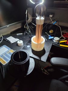
We have been behind schedule for weeks. And technically, here at the end of official work time, we still are by about a week. What remains is final integration and assembly. However, we do not intend to stop just because the final presentation is this coming week. As such, tomorrow, we will be doing final integration items, in hopes to include a success result in our presentation, and certainly our final demos.
By the end of this coming week we will have it fully assembled, and hopefully we will successfully have achieved our MVP.