
Since the week before was busy with getting the long design report done, I unfortunately didn’t have time to work on the PCB. (I did watch some tutorials about how to design custom components, because Fusion360 conveniently doesn’t have the Beetle and microphones in any library package that I could see.)
First step was to create a circuit diagram using better tools than powerpoint (because those diagonal arrow lines were a bit chaotic to read). I used draw.io, which isn’t perfect with customizability options, but I’ve used it before and it integrates with Google Drive so that’s a plus. Here is the picture: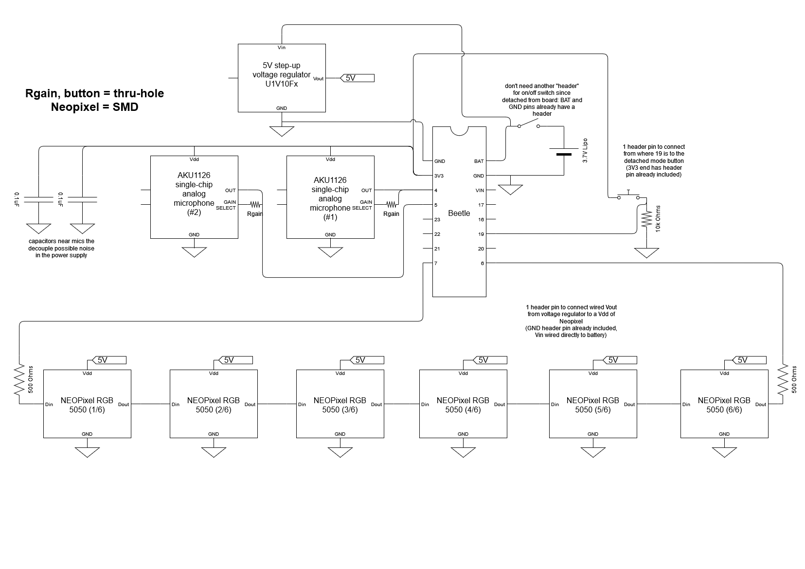
Isn’t it beautiful? Changes from the design report picture include the capacitors near the mics to decouple noise from the power source, as well as resistors for Din and Dout of the Neopixel chain. Finally, there are some notes about header pins because some components are floating off the PCB board, and will need to be connected by wire, so header pins would be a good attachment method.
Now time for the PCB. Thanks to this video [https://youtu.be/NITJZfhjppI?si=aJQx4koncQ27g8tM] I learned how to make components based on the data sheet to add to my custom library. Another hiccup was that Beetle didn’t have detailed dimensions on its datasheet, so I had to infer the measurements by finding the male header pins datasheet instead. Luckily the microphone had a beautiful datasheet, but the next problem was the grid granularity, which meant I could only place solder pads at certain distances; I calculated the centers of the mic pads were about 1.1mm apart, but the grid size was at 1.27mm (and it’s not recommended to change the grid size to be compatible with manufacturers). Prof Fedder said it would probably be ok to just leave the pads at that distance. This grid granularity also affected the placement of the components, so they wouldn’t be at the exact same distances that the Solidworks render was at, but they were generally in the same place.
Yet another problem I ran into was the “polygon pour”, where hypothetically an entire side of the PCB would be at 3V3, or GND, so it would make the power and GND traces a lot shorter and more convenient. Unfortunately, Fusion360 was acting up again and refused to recognize traces that should’ve been connected, so I ended up needing to manually wire all of those as well. Those traces were widened from the default of 0.254mm to about 0.6mm because they needed to be longer (to mitigate resistance and heat), and the traces that had to cross the Beetle’s width were widened to about 0.4mm. These were just what I thought would work instead of doing rigorous calculations. Katherine checked the calculations and said they would be fine. Here’s another picture:
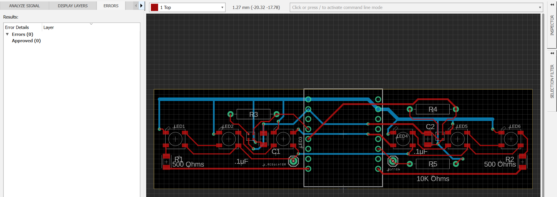
Wow, so beautiful. That took several days of feedback cycle to get done! Thus, the Gaant chart has been updated to show the prototyping stuff due a week later. While we wait for the PCBs to come in, I will help with the ethics assignment, and perhaps try experimenting with the Beetle. The PCB should be coming in within the week though, so perhaps I will have a chance to solder things before the next status report. This will also depend on when we can pick it up and when the PCB lab is open.
*if the images are blurry then I’m really sorry WordPress is doing that, I swear the original images are crisper and Google wasn’t super helpful.
Here are links:
Circuit diagram: https://drive.google.com/file/d/1MFEq_3fogkLBO0vlU_rchOyh7q9sXybE/view?usp=sharing
PCB: https://drive.google.com/file/d/1XLOiJtNyhyGow_l14J2nMGxhX-5LmUrL/view?usp=sharing