Significant amount of time was spent working on the design report this week, including FPGA implementations, diagrams, and overall project information.
Began coding modules for clock dividers that will be needed to time UART communication on the USB transceiver and laser side.
Came up with block diagram for the transceiver, consisting of 2 shift registers that will be enabled depending on number of bits that go into each.
Schedule
Design report took more amount of time than originally thought. Implementation will need to be worked on, which will hopefully be done the week after spring break.
Next Week
Have an overall implementation of all aspects of the FPGA, so that debugging can be conducted the week after using oscilloscopes for signal accuracy
The biggest remaining hardware risk is that the FTDI circuit is incorrect. If it is, we will be unable to communicate with the FPGA board through it, and we will not be able to draw 9V from the USB connection. Our mitigation plan for this was to model the circuit as much as possible on a manufacturer created reference design, and to ensure we will be able to make the project even if it fails. This will be done by communicating with the FPGA board through its native USB or through an external UART-USB adapter, and powering our board with a 9V power supply connected separately. This will allow the project to function even if the USB plan does not work.
Design Changes
The lasers have been shifted to both be powered off of 9V rather than IR being 5V for consistency and ease of debugging.
We added a 3.3V LDO to our custom board powered directly from 9V rather than relying on the one on the FPGA board powered by 5V. This is because the FTDI chip requires a 3.3V power supply, and since USB defaults to 5V, the FPGA board will be supplied 5V minus the dropout voltage of our LDO, which is about 1. We cannot guarantee that we will get the 3.3V back from that board that the FTDI chip needs in order to operate (and request 9V), so we need to have a way to get 3.3V reliable from the usb power regardless of voltage.
We connected all interface pins from the FTDI chip to the FPGA GPIO so that we can decide to switch interfaces later, rather than being locked in to the one we pick before ordering the PCB.
Updated Schedule
We have no major schedule updates. We were able to test our lenses ahead of time, so no longer need to do that next week.
Progress
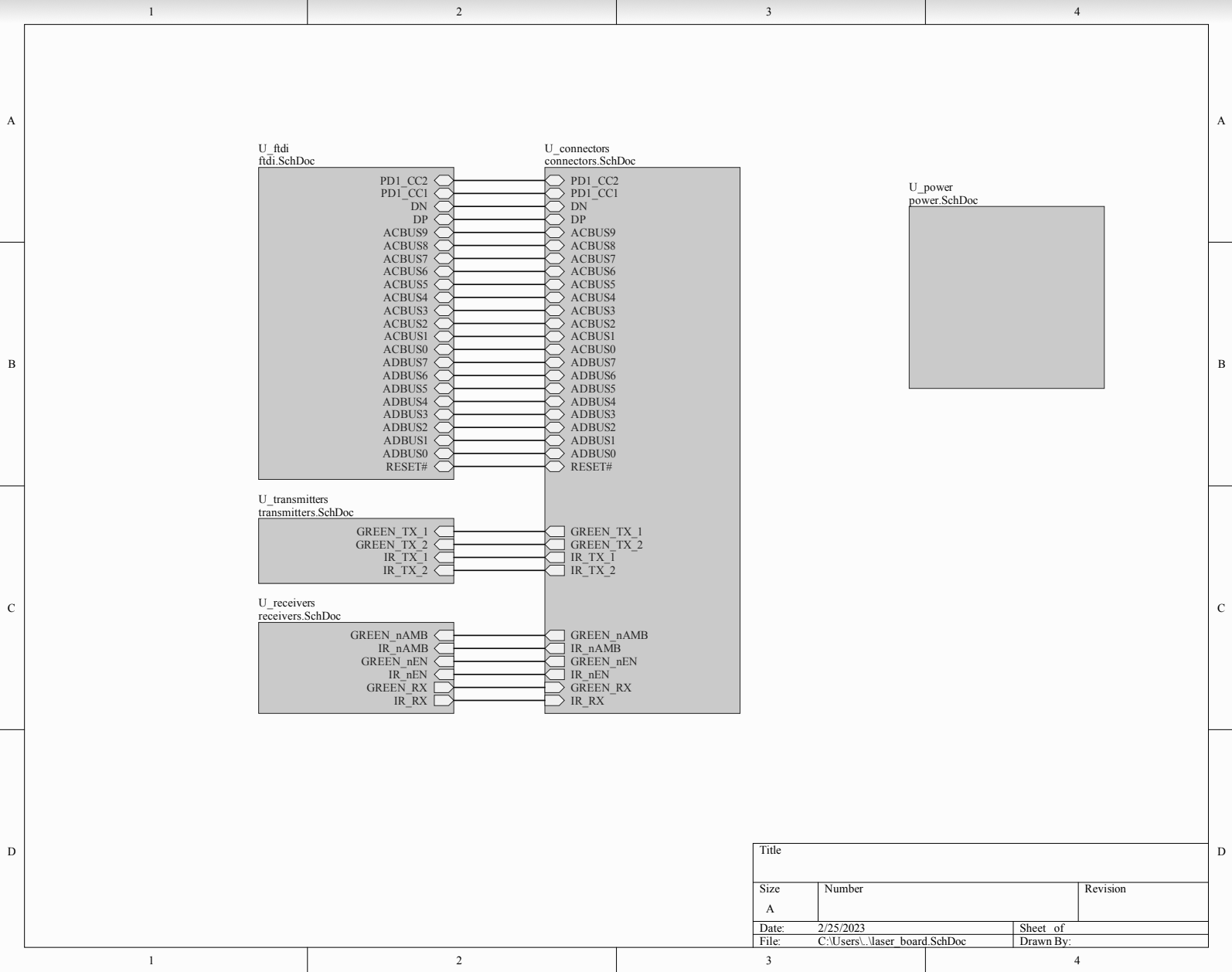
Our schematic is complete! Full schematic is located here and is 6 pages.. Below is the front sheet showing interfaces between different subsystems.
The laser beam focus was one of our concerns, as we tested the beams last week and it was very wide angle. We tested out the laser again this week using empty laser housing that we ordered, and the beam was focused very well.
Before:
After:
Team Dynamics
There hasn’t been team issues working on our project.
We have shifted some assignments so that each person has work to do. Initially, we weren’t sure if we would have signals aspects in our projects, because we considered the use of DSP to clean out the signals that we get. However, because we realized that there were complications using the ADC (sample rate), etc. we have decided to use comparators instead. If we were to implement this, Roger would have dealt with the signals. Instead, we moved some of the EEPROM configuration to his task. In addition, due to communication protocol difficulties that we might face, we also shifted the Hamming encoding/decoding to him as well.
There was also a need for 3D printing that didn’t occur to us in the beginning. This has been taken on by KJ, since it would probably be easiest for him to interface with the PCB, and there will be more software/programming implementation for the rest of the team later on.
Presented the design review for our team on Wednesday.
Worked on slides and practices beforehand.
Thought further about FPGA implementation, especially with regards to the interface between the FTDI chip.
For the FTDI chip, I had some concerns about using a single fast serial data that splits into 2 serial data complicating timing. As a backup plan and knowing options, I looked into potential other modes that the FTDI chip supports, and found the asynchronous FIFO mode. This was the only other option that seemed reasonable to use, as others supplied a 60MHz clock (faster than the FPGA onboard and will probably not go through the GPIO pins smoothly). I plan on attempting to implement the FPGA with the fast serial, but as a backup go into FIFO if there are timing issues that become difficult to smooth out. In addition, if speed of the fast serial becomes a bottleneck, this can also potentially allow for a much faster interface between the FTDI buffer data and the FPGA.
Thought through a little more of the block diagram and overall implementation, especially before the hardware arrives.
My plan is to have a rough implementation of the FTDI side, since some aspects are difficult to predict without the actual hardware in hand. I plan on working and refining more of the actual laser side since that can be read with the oscilloscopes through the GPIO headers to verify actions.
Helped focus the laser to verify that the laser beam angles can be fixed.
Overall schedule
I think that this week’s primary focus became the design review for the first few days. Although it’s not very far off schedule, I think that I could have worked on a more detailed implementation of the FPGA, which I plan on doing next week instead.
Goal for next week
Have an implementation of the laser side, and a rough idea of how the interface would be handled on the FTDI side on the FPGA.
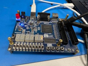
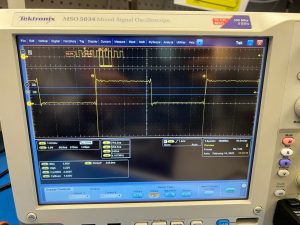
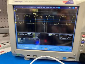
Tested speed of FPGA I/O pins from the Dev board to see how fast communication can go from custom PCB to the FPGA
Measured that 12.5MHz clock can cleanly be measured from the GPIO pins. From this, we decided that using an FPGA dev board was sufficient and a better option than a microcontroller. Faster speeds yielded questionable results, although there is a possibility that the oscilloscope probes couldn’t measure as fast. We can safely rely on using the 12.5MHz clock (i.e. 25 Mbps) communication for our project.
FPGA Spec
50MHz clock
3.3V active high from GPIO pins
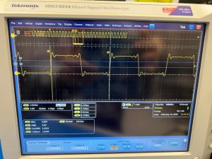
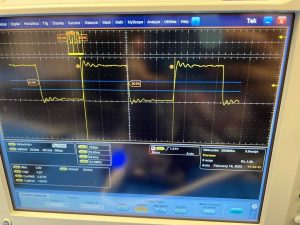
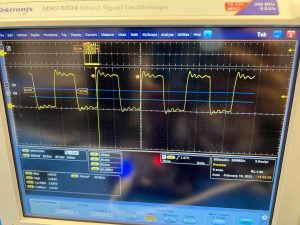
Detailed measurements:
4.15MHz from FPGA, measured with an oscilloscope at 500MS/s sampling:
Worked with Roger and KJ to come up with communication protocol.
We weighed the different options between a SPI-based and a UART-based protocol, and concluded that we will use a UART-based protocol for LaserDrop, as this would yield better results after evaluating it while thinking about sampling speed from FPGA, circuit response, etc.
Decided on the packet properties of the laser communication (start sequence, packet ID, data, Hamming encoding, packet size)
Decided which aspects of our project (CPU, FPGA, circuits, COTS IC) would handle which part of the protocol
Came up with an error handling mechanism for lost packets
Came up with a handshaking mechanism for beginning/end of instantiating a communication
Designed the FPGA block diagram that would handle this communication.
Overall FSM and block diagram that will interface with the FTDI chip and PCB circuitry.
Worked on the design review presentation with the whole group.
Schedule
My work is on schedule. My goal last week was to test whether the FPGA dev board or the microcontroller would be able to support the communication, which I was able to do. Due to the success of how fast the signals came across from the FPGA board, we concluded that a microcontroller would be unnecessary and we can go forth with a custom PCB that would interface with the FPGA.
Goal for next week
Practice and present the design review during class.
Address the feedback/concerns that we receive during the design review from the advisors, faculty, and classmates
Refine and come up with a detailed FSM/block diagram of the whole system
Principles/Courses Used
18-240, 18-341: In these classes, I learned how to use and design the FPGA boards (Altera DE0-CV), which I used to think about how the FPGA will interface with the FTDI chip and PCB circuits and handle the protocol that we designed. In addition, protocols such as the Hamming encoding and USB were explored in these classes that helped when we were coming up with the communication protocol. In addition, I wrote simple SystemVerilog code to test out the FPGA speeds, which I will heavily use later on in this project as well.
18-349: Embedded Systems taught about various protocols such as SPI, UART, and I2C that we thought through while coming up with our custom protocol. In addition, 18-100 and Manchester encoding, etc. were another features that we thought about when thinking about the communication protcol.
MoonRanger (16-861/16-865: Space Robotics): Gave me hands-on experience with communication protocols (UART, etc.) that helped during protocol design. In addition, I learned and often used oscilloscopes and other tools, which made it easy for me to figure out the FPGA speeds.
Searched for FPGA/microcontroller options that were available for purchase
Found out that FPGA chip on a custom PCB would most likely be a difficult option. I was restricting the search to Altera chips (and non-BGA if possible), and found that most chips were out-of-stock or too old so that any recent version of Quartus does not support this.
The search was restricted to Altera due to my prior experience in 341/240.
Looked into a microcontroller that would have UART/SPI, that would enable communication from the FTDI (USB-UART chip) to the lasers. Filled out a purchase form for a MSP430 Launchpad. Estimated day of delivery was Monday if it were ordered yesterday.
KJ and I both have experience using MSP430 in the past, which is why we narrowed down the search to this.
We decided to get a dev board to test out its capability so we can make sure that it can support at least the 4Mbps communication to meet requirements.
Work is on schedule, although the unavailability of FPGA chips were unexpected and I would need to iron out the plan of handling the communication.
By next week, I hope to come up with a way to validate whether the microcontroller and FPGA dev board can support the communication requirements, and choose which design to proceed with based on this.