
Anju Ito’s Status Report for 4/29/2023
- Work this week
- Work on most of the Final Poster. Create diagrams and contents.
- Start creating and writing the final report, copying from the design report and starting to document changes.
- Help with and keep up with the software testing happen, although FPGA code has not been touched for software to debug.
- Final presentations during class.
- Schedule
- We are on track with the schedule. What remains are mostly final documentation work for the demo and report, as well as fine tuning for me. Software bugs has mostly been sorted out.
- Next Week
- Finalize final poster, and create final report/design. Most of the technical design has been done last week, so what remains are the final documentation, and potentially testing different communication speeds/minor encoding to get the last speed boost out.
Team Status Report for 4/29/2023
- Risks
- The USB driver crashes when reading occasionally. This happens frequently enough to prevent us from transmitting large files. We are not sure why this happens yet. We plan to look into this bug and hopefully find what is happening. If we do not figure it out, we will try to have the code try to reload the USB Device repeatedly if it happens. Updates to fpga code seems to stop this from happening. We can now send large files without this ever happening.
- The software sometimes goes into a deadlock when both receiver and transmitter has data on its TX buffer. The timing and acknowledgements is hard to get right, but we may make some assumptions to make this work.
- Design Changes
- No design changes this week
- Updated Schedule
- We are on schedule to finish the final deliverables (poster, report, and video). We still need to run our system stress test which will be done soon.
- Progress
- We have nearly completed our poster, which only needs a final review before submission.
- Unit Tests
- Laser Speed Test
- Use FPGA to transmit set signal over lasers. Measure the receiver inputs into the FPGA using an oscilloscope
- Results: Measured clean 6.25Mbps with proper focus
- Findings: The fall time was much slower than the rise time, especially when the receiver was getting too much focus (up to 120ns). This made it important that the focus is adjustable and set correctly, and slower transmission speed more desirable than faster.
- Power Test
- Measured power draw with all components on.
- Results: 0.223A draw from 9V power supply
- The USB-PD can support up to 9V for 3A, which easily passes our criteria.
- Ambient Light Test
- Laser transmission tested in multiple rooms, to ensure that most room settings are fine for transmission.
- Results: The laser worked similarly and properly under all room conditions.
- USB Speed Test
- Ensure that USB can transmit to our PCB that would meet the use-case transmission requirement
- Findings: The baud rate set at 7 Mbps is working, which passes the test.
- Angular Error Test
- At 1m, measure the largest laser focus that transmits properly.
- Results: Calculating the angle of error based on the target size, we found that the angular error can be +/- 0.13 degrees in minor direction, and +/- 0.32 degrees in major direction.
- Findings: The focus that would make this system work had a much smaller target than we originally anticipated, since the receivers produced much less current than calculated based on the datasheet. We lowered our use-case requirements to adjust for this. In addition, we added handshaking between each packet to make sure that packets aren’t continuously transmitted even when the aim is off.
- Error Correction Test
- Tested Hamming code error by injecting 1-bit and 2-bit errors.
- Results: The test passed, with the software correcting 1-bit errors and reporting that there were errors for 2-bit errors.
- FPGA Communication Test
- Had the transmitter FPGA receive data over USB, send it to the receiver, and the receiver checks for the start sequence and begins to write the data into the FTDI chip after receiving a full 1kB. Timed this using counters in FPGA. Not use lasers, and communicate by connecting receiver/transmitter FPGA via jumper cables.
- Results: For a given transmission speed (6.25Mbps), data sent 97 percent of the time, with other 3 being taken up by FPGA processing (6.06Mbps of throughput), that will be even more amortized if more packets are sent. Pass requirements.
- Laser Speed Test
- Integration Testing
- Device Speed Test (without USB)
- Time the FPGA transmission of usable data from the moment it arrives at the FTDI chip to the moment the receiver FPGA attempts to write to it.
- Results: 2.21 Mbps of usable data observed at 4.47 Mbps of transmission. This is after taking away the overhead put on from UART (8 data bits / 10 bits), Hamming (11 data bits / 16 bits), and protocol overhead (packet starter and packet tag).
- System Speed Test (with USB)
- Timed transmission of one packet to another using a laptop
- Results: Observed ~2 Mbps of usable data, meeting the adjusted 1 Mbps required.
- File Send Test
- From close distance, send a small (< 128kB) file from one device to another.
- Results: Packets delivered properly and reconstructed!
- System Stress Test
- Put full system together, and send one large file (19MB) to the other at a distance of 1m.
- Result: File sent correctly!
- Device Speed Test (without USB)
Anju Ito’s Status Report for 4/22/2023
- Work this week
- Finalize laser transmitter/receiver and FTDI interface
- All inputs go through 2 flip flops to avoid metastability
- Better timing for all I/O devices
- Implement handshaking
- Handshaking occurs before every packet send now
- Series of 0xAA sent by transmitter. Receiver responds with 0x10
- Implement packet sending/receiving
- Sender: send bytes in 1kB chunks. Handshakes before each one.
- Receiver: receives bytes. If receive < 128kB after handshaking, will pad out the bits with all 1’s
- Use 128kB buffer on receiver/transmitter
- If more than 1kB sent/received, FPGA has capability to store that.
- Created to accommodate for slow USB transmission.
- Create Manchester/Duty-cycle like encoding for FPGA
- Made the last half of each bit a 0. We found out during testing that the ambient light filtering would adjust to the laser light level if we were transmitting a lot of 1’s in a row. In order to mitigate this, we made half of each bit a 0, and sample on the first half.
- FPGA Cycle Counter
- Added debugging counters to report how many clock cycles packets stay on the FPGA.
- Measured from the point that the transmitter FPGA saw data on the FTDI chip until the receiver FPGA received and put the data onto FTDI chip.
- Debugged a lot of FPGA code using setup where FTDI code was connected to the FPGA, and laser receiver/transmitter connected via jumpers to each other.
- Finalize laser transmitter/receiver and FTDI interface
- Schedule
- We are cutting into slack, but the core part of the project is done. We have moved onto integration and testing. In terms of work, this has transformed into adding/getting rid of debugging features for testing and design trade-offs. We have successfully transmitted a large file (19MB) over lasers, and reached MVP!
- Next Week
- Continue working on integration. See the best methods of transitions and talk about design decisions at full-scale level. Refine.
- Work on design report/poster/presentation.
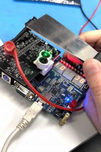
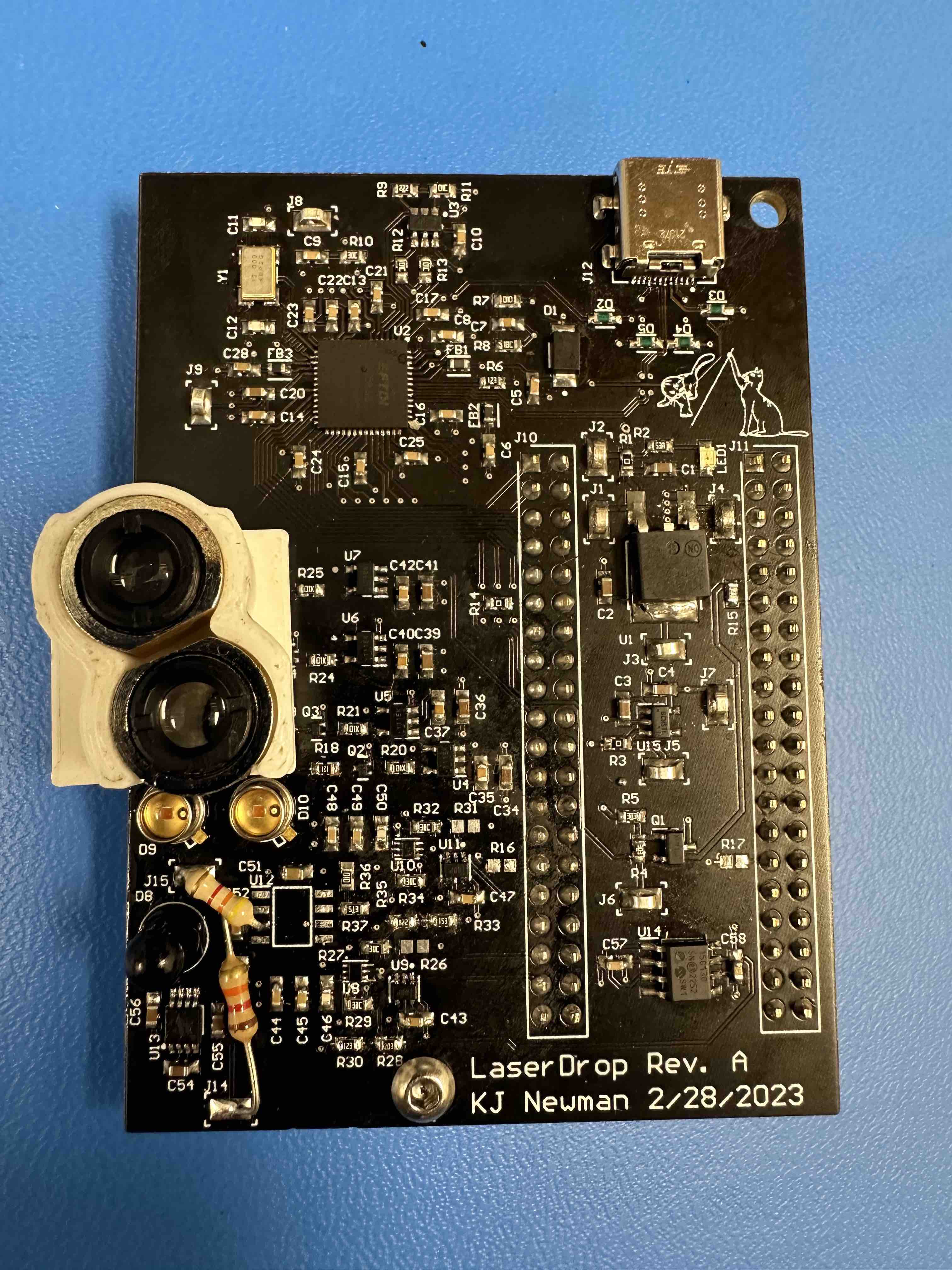
FPGA setup used for debugging
Anju Ito’s Status Report for 4/8/2023
- Work this week
- Integrated RAM use on the FPGA. Created a 1k FIFO using Quartus IP, and successfully integrated into the code. This fixed the error of not having enough logic components to compile the design on the FPGA, and instead using the embedded RAM on the chip.
- Fixed a FSM logic bug that prevented the FPGA from transmitting 2 bytes in a row over the lasers.
- Fixed timing issue for writes onto the FTDI chip. When testing with lasers, occasionally saw that the 6th bit in the byte was always a one. There was a logic error in the setup time that resulted in data not being held for an appropriate length before the write was asserted.
- Finished writing code and loading all the files for demo. Created a board that can be configured to echo just using the FTDI chip and back, and another that transmits whatever it receives through the USB on the laser and writes back whatever it sees on the receiver back to the USB. Also attempted to test by turning the lasers completely off and on, board-to-board transmission (worked much more poorly then single board using mirrors), and turning ambient light filtering off (not work too well).
- Attempting to fix the board-to-board by creating mounts for the PCB so that they are more stable.
- Working through making the receiver more robust. Cleaned out logic, which may have made it slightly better. However, still occasionally see duplicates in numbers during laser transmission, which needs to be fixed/explained.
- Schedule
- Everything that we prepared for the demo we were able to show, although there are new issues such as the necessity of extremely precise alignments and receivers having errors that need to be addressed in the future. Everything is around 2 weeks behind schedule, as implementation is taking a longer time than planned.
- Next Week
- Attempt to make laser transmission code more robust. Currently seeing duplicates and wrong bits too regularly.
- Potential solutions: Fix any bugs that exist, slow down transmission speed from 6.25MHz, change how the receiver is sampling, add real-life flaws onto simulation to attempt to get error, 3D printed mounts
- Implement handshaking protocol.
- Work with integration and start testing.
- Attempt to make laser transmission code more robust. Currently seeing duplicates and wrong bits too regularly.
- Testing/Verification
- Unit Tests
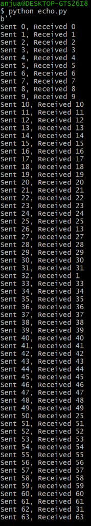
- Echo to test FPGA/FTDI/computer connection: Test that verifies the connection between FPGA to computer by computer writing/reading bytes, and the FPGA echoing that back through the FTDI.
- Verified. Attempted to time, and realized that computer’s read function especially takes a long time to run, but the number of bytes read doesn’t affect speed.
- Laser transmission test: Verifies that the whole pipeline from computer to FPGA to lasers work with single byte.
- Verified. However, alignment changes results a lot, and multiple bytes become less stable.
- Packet send test: NOT DONE. Send a full packet, and verify that it was received correctly on the other side. Should not load it onto the FPGA if the start sequence is not received properly.
- Echo to test FPGA/FTDI/computer connection: Test that verifies the connection between FPGA to computer by computer writing/reading bytes, and the FPGA echoing that back through the FTDI.
- FPGA Integration Tests
- Stress Test: fill FTDI chip multiple times, see if it can process data appropriately
- Speed Test: measure pin out speed with oscilloscope to verify laser transmission
- Light Test: Try testing in different lighting environment to see that transmission works under reasonable room conditions
- Distance Test: slowly move the boards away from each other. Adjust focus, and record the max distance bytes can be transmitted at.
- Unit Tests
Demo
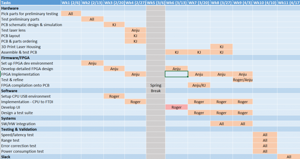
Updated Gantt Chart:
Team Status Report for 4/1/2023
- Risks
- IR seems to use incompatible photodiodes and receivers. We do not have a way to fix this, so we will just not use it. This was always a risk, and a big part of the reason we made sure to have multiple lasers was in case one did not work.
- Design Changes
- We are now using a usb power/data splitter for our usb cable. This allows us to use a usb pd source, like a wall charger, for power, combined with usb 2.0 data from a laptop. The board combines them into one cable for use on our board.
- We are now only using the green laser. IR hardware does not work, but green does. The green also appears potentially fast enough to meet our requirements on its own.
- The charge pumps are creating very large radiated emissions onto our photodiode traces. To deal with this, we are using only the charge pump which is further away from the green photodiode. This is far enough to not introduce noise onto the line. This is done with some resistors attached on top of the board, and the regular charge pump DNP’d.
- Updated Schedule
- We will continue working on integration for the next week and beyond as more subsystems are ready to work together.
- Progress
- The power splitter board came in, was reworked, and successfully delivered both power/data to the PCB. This splits the USB-C line from the PCB into power and data outlet, which can be connected separately to a power supply and a computer.
- The data path from FPGA to laser back to the FPGA was successfully verified at a speed of 6.25 Mbaud, even over just 1 laser!
- The board hardware is seemingly complete!
Anju Ito’s Status Report for 4/1/2023
- Work This Week
- Wrote an echo program that reads bytes on the FTDI, and writes them back so it can be tested with computer software. Some bug exists with the reading, but communication has been established and it was seen that correct bytes can actually be read and written from the chip from both directions.
- Continued to debug the FSM. Transitioning over to building smaller modules.
- Attempted to transmit data at 6.25 Mbaud through laser. Sent it over FPGA, and received correctly on the board! Some bugs about reading, but verified that a single bit width can be detected and read.
- Attempted to compile the Echo, and realized that 512 bits couldn’t be declared. Because that was the intended size for packets, realized that this needs to use built-in embedded memory on the FPGA, and created an IP that may be integrated and used instead. This can hold kbytes of memory, which is more than sufficient for our application.
- Schedule
- We were successful in verifying that both sides (lasers and FTDI chip) work to and from the FPGA. Next steps include debugging and building a more robust system, as well as integrating it into the full system. Things are behind schedule, partly as integration requires different projects and modules, which slows progress of FPGA development because they are not as modular as software.
- Next Week
- Figure out a code to put on the FPGA board during the demo
- Make the memory work for the FPGA.
- Fix bug for read write on FTDI.
Anju Ito’s Status Report for 3/25/2023
- Work This Week
- Designed, programmed, and compiled the FPGA FSM and datapath, though it needs much debugging work.
- Got the simulation to run and wrote a testbench. The testbench did not work for a while due to syntax issues with ternary operations, but runs now and there are issues to debug.
- Helped look at EEPROM programming to set the chip to 245 asynchronous FIFO mode using 9V 3A power delivery.
- Schedule
- The code is slightly behind schedule, and I hope to finish debugging the FSM through simulation by this week so that integration goes smoothly by the end of this week or next week.
- By the interim demo, I hope to have a working FPGA code written. Although this cannot be demoed unless an FTDI chip and computer software is written. The basic sending data and receiving may be demonstrated as MVP.
- Next Week
- Finish debugging the full FPGA code through simulation.
- Help out in other tasks as necessary, and possibly integrate with code/FTDI chip/lasers.
Anju Ito’s Status Report for 3/18/2023
- Work This Week
- Began to write FPGA code. Progress:
- Wrote a laser transmitter module that will transmit 2 input data over 2 lasers if the data valid signal is set. This module will always transmit both data simultaneously. This is the desired behavior for the project, as our MVP will never use one laser and not the other.
- Wrote a laser receiver module that always listens for a byte that follows UART protocol (start bit and stop bit). This module was configured so it can only receive both at the same time, and currently making different versions to test the receiver.
- Debugged the laser transmitter and receiver by setting up the waveform viewer environment. This took some time, as the vcs compiler kept exiting on failure. It turns out that the source bashrc has to be called every time, and I have to make sure that I only have setup447 (or one of the class) and not the other, as those conflict with each other now.
- Wrote an untested version of the FSM and protocol handler of the transmitter module.
- Verified functionality of the transmitter and receiver modules by sending constant bytes from the transmitter to receiver using a single board, connected by jumper cables from the laser out line to the laser in line. Successfully sent bit, flashing the data received every time, and allowing for switches.
- Imported pin configurations and assigned appropriate ones based on schematic. Modified code so that all GPIO pins except for transmitting and outputs are high impedance, and labeled/used each one for its set purpose.
- Flashed the code successfully onto FPGA non-volatile memory. This involved emailing/creating a Terasic account to get their programmer, and converting file formats. This makes it much easier to just turn on the device without needing to reconfigure the board every time.
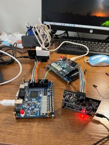
- Integrated the FPGA with the PCB. Fixed issues with DNP resistor labelling that caused the FPGA to be turned partially on (3V3 was connected instead of the 5V to the FPGA. Fixed by removing and putting on the resistors). Verified that the lasers can be somewhat controlled by the FPGA, although there is no way to test it so far as the receiver did not work with preliminary testing using mirrors.
- Began to write FPGA code. Progress:
- Schedule
- Things are on schedule. Since boards have arrived and KJ has assembled them, my implementation from now will most on likely work in parallel with testing the board features and making sure that they will work. This will involve modifying the code and making a simplified version of it which would take some time, but also ensure that the code will work well with the board.
- In addition, since there are potential issues with the receiver and we need to verify the functionality of the lasers, etc. I will use some time attempting to write test code and debugging that feature, which may slow down me working on FSM.
- Next Week
- Write out the full program for FPGA including the receiver FSM, and testing the transmitter FSM. Integrate it with the board and see how far I get.
- Test out the laser transmitter/receiver on the PCB, because integrating with the FPGA may be the easiest way to test the board functionality, since it receives high speed transmission. Since it didn’t register the first time transmitting at 6.25 MHz using a mirror, potential things to do are slowing down this transmission speed greatly, using 2 boards for better laser power going to the other board, turning off ambient noise cancellation, and testing in a dark room.
![]()
Bits being transmitted and received by the receiver module (displayed on the HEX values, the first 2 for the IR receivers and the second 2 for the green receivers). The GPIO pins are connected with jumper cables.