My major tasks this week included:
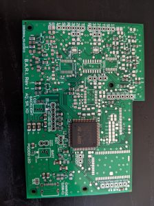
REV 1 PCB BRINGUP: Our PCB boards for Rev 1 (pictured below) arrived Tuesday, and the components to populate them arrived mid-day Wednesday. Before the arrival of these parts, I compiled a several page PCB Bringup Procedure (part of the larger BARI Test Procedure) to describe the final electrical manufacturing and test of these boards. After the parts arrived, this document guided me as I assembled our first testboard (“Bernice”) and worked with Xingran to validate different sub-sections of the design.

Two significant setbacks occurred in this process: First, JLCPCB failed to populate many of the SMD passives on our board. (They have since offered a refund for those components.) Second, I made a series of soldering mistakes that rendered Bernice’s ADC unusable. Nevertheless, we managed to bring up the STM32 microprocessor, communicate on the I2C bus, and verify that the BM83 is functional.
BARI BOX: Simultaneously, I started the design of the BARI BOX, the mechanical enclosure which will enclose the BARI PCB and provide a mounting place for all of its components. I will refrain from posting an image of the WiP BARI BOX so as to not spoil the surprise ~~~
In response to the glitches above, I’ve formulated a revised hardware plan that calls for creating a second Rev 1 (“Alexey”) in the coming week, using newly-ordered components and revised soldering procedures. Rev 2 fabrication will be somewhat delayed relative to our schedule to allow for sufficient testing on Alexey. My current target is to order the Rev 2 boards by 4/8 (and receive them by 4/18).
