
REV 1 SCHEMATICS: I completed the schematics for Rev 1 and sent them out for review on Monday (3/1/2021). The response from our reviewers (our TA and advisor) was mostly positive, but our TA identified a new ADC component which could offer superior performance over our existing solution, which led me to redesign the input stage with input from my teammates and our advisor on Thursday/Friday. The new input stage features a 4-channel audio ADC which communicates with the microprocessor on SPI and a new audio-class amplifier for the preamp block.
REV 1 LAYOUT: In parallel with the above, I began laying out the Rev 1 PCB board. Rev 1 is a mixed signal board including both audio and RF signal paths, as well as moderate-frequency digital signals, necessitating care in layout.
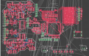
As can be seen in the image above, I’ve finished internal layout for most of the main blocks, including the Analog Effect, LCD bus, and BM83. Most of the Power Module and part of the UI module remains to be routed, but I expect that I am close to completion because the routing for these remaining components is less complex than what I have done so far.
DESIGN REVIEW PRESENTATION: I will be delivering the design presentation next week, so I have been working together with my teammates to create the slides and understand the content I need to present, which includes substantial work that was not done by me. We plan to hold a dry run presentation on Sunday before the slides are due.
I had previously hoped to finish the layout and order the board by the end of this weekend. However, due to the late redesign with the ADC, it seems more realistic to let this deadline slip by a few days and order the PCB before Wednesday. Finishing the layout and all of the associated tasks necessary to order this PCB will be the main focus of my effort in this coming week, along with participating in the design review process. Overall impact of this change on our project schedule should be minimal.