Theodor’s Status Update for Mar. 28

Accomplishments

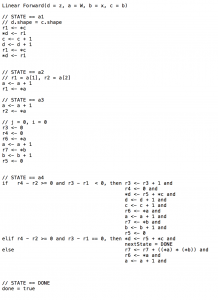
This week I accomplished one of the hard parts of the FPU job manager: writing the FSM for the Convolutional Forward module.

It’s worth mentioning that there were easier options for implementing Convolutional Forward than to define the operation in an FSM. We could have chosen to write convolutional forward in C, compile it to RISCV-assembly, and copy the code to our FPGA and use that, but this would require precious on-board memory that we need to store input samples. Writing Convolutional forward as an FSM is the fastest and smallest solution to our problem, and doing so will maximize our model throughput. Convolutional backward (gradient with respect to the inputs, filters, or bias) are essentially the same nested loops above, so implementing those operations will be significantly easier if I use the code above as a starting point.

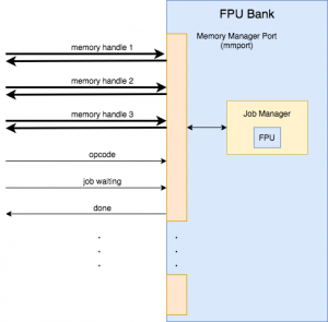
I now know the exact requirements that the FPU Job Manager needs: 32×32-bit registers that can be accessed with multiple reads and multiple writes per cycle (I will have to declare an array of registers and expose all of the wires instead of writing a Register File), and some specific ALU/FPU instructions:

  • offset = channel_index + (num_channels * i) + ((num_channels * image height) * j)
  • x = x + 1 (integer increment)
  • x = y + z (integer addition)
  • floating-point multiply
  • floating-point addition

Like I mentioned last week, having Convolutional Forward completely defined will cause a lot of other pieces to fall into place. Next week, I plan on implementing some of these ALU/FPU and register requirements in SystemVerilog.

Here’s what my definition looks like:

pseudocode:

w_o_fac <- x.height * x.channels

j <- 0
j_x <- (-1 * pad)
while(j < z.width):
  w_o <- w_o_fac * j_x
  i <- 0
  i_x <- -1 * pad
  while(i < z.height):
    beta <- 0
    while(beta < f.width):
      alpha <- 0
      while(alpha <- f.height):
        gamma <- 0
        while(gamma < f.in_channels):
          delta <- 0
          while(delta < f.out_channels):
            z[delta, i, j] <- z[delta, i, j] + (f[delta, gamma, alpha, beta] * x[gamma, i_x + alpha, j_x + beta])
            
            delta <- delta + 1
          
          gamma <- gamma + 1

        alpha <- alpha + 1

      beta <- beta + 1
      
      delta <- 0
      while(delta <- z.channels):
        z[delta, i, j] <- z[delta, i, j] + b[delta]

        delta <- delta + 1

    i <- i + 1
    i_x <- i_x + stride

  j <- j + 1
  j_x <- j_x + stride


State transitions:

// STATE == START_LOAD1
r1 <- stride
r5 <- filter.output_channels
r9 <- x.height
nextState = START_LOAD2


// STATE == START_LOAD2
r2 <- pad
r6 <- filter.input_channels
r10 <- x.width
nextState = START_LOAD3


// STATE == START_LOAD3
r3 <- output_height
r7 <- filter.height
nextState = START_LOAD4


// STATE == START_LOAD4
r4 <- output_width
r8 <- filter.width
*z <- output_height
z++
nextState = START_CALC


// STATE == START_CALC
*z <- output_width
z++
r11 <- r9 * r6         // w_o_factor = x.height * x.channels
r12 <- ~r2 + 1         // j_x = -1 * pad
r19 <- 0               // j = 0
nextState = J_LOOP


// STATE == J_LOOP
r13 <- r11 * r12
if(r19 == r4):         // if j == z.width
  nextState = DONE
else:
  r21 <- 0             // i = 0
  r20 <- ~r2 + 1       // i_x = -1 * pad
  nextState = I_LOOP


// STATE == I_LOOP
if(r21 == r3):         // if j == z.height
  r19 <- r19 + 1       // j += 1
  r12 <- r12 + r1      // j_x += stride
  nextState = J_LOOP
else:
  r22 <- 0             // beta = 0
  r28 <- r20 * r6      // r28 = f.input_channels * i_x
  nextState = BETA_LOOP


// STATE == BETA_LOOP
if(r22 == r8):         // if beta == f.width
  r25 <- 0             // delta = 0
  z <- z - r5          // Reset z counter, we’re going to iterate over channels again
  b <- 2
  nextState = BIAS_LOOP_LOAD
else:
  r23 <- 0             // alpha = 0
  nextState = ALPHA_LOOP


// STATE == ALPHA_LOOP
if(r23 == r7):         // if alpha == f.height
  r22 <- r22 + 1
  nextState = BETA_LOOP
else:
  r24 <- 0             // gamma = 0
  nextState = GAMMA_LOOP


// STATE == GAMMA_LOOP
if(r24 == r6):        // if gamma == f.input_channels
  r23 <- r23 + 1      // alpha = 0
  nextState = ALPHA_LOOP
else:
  r25 <- 0            // delta = 0
  r27 <- r24 + (r6 * (r20 + r23)) + (r11 * (r12 + r22)) // x offset
  nextState = DELTA_LOOP_LOAD


// STATE == DELTA_LOOP_LOAD
r14 <- *z             // r14 <- z[delta, i, j]
r15 <- *f             // r15 <- f[delta, gamma, alpha, beta]
r16 <- *r27           // r16 <- x[gamma, i_x + alpha, j_x + beta]
if(mem(z).done && mem(f).done && mem(x).done):
  nextState = DELTA_LOOP_CALC1
else:
  nextState = DELTA_LOOP_LOAD


// STATE == DELTA_LOOP_CALC1
  r17 <- r15 * r16    // r17 <- f[delta, gamma, alpha, beta] * x[gamma, i_x + alpha, j_x + beta]
  nextState = DELTA_LOOP_CALC2


// STATE == DELTA_LOOP_CALC2
  r18 <- r14 + r17   // r18 <- z[delta, i, j] + (f[delta, gamma, alpha, beta] * x[gamma, i_x + alpha, j_x + beta])
  nextState = DELTA_LOOP_STORE

// STATE == DELTA_LOOP_STORE
*z <- r18
if(mem(z).done && r25 == r5): // if(memory is done writing and delta == f.output_channels)
  r24 <- r24 + 1
  nextState = GAMMA_LOOP
else if(mem.done):
  nextState = DELTA_LOOP_STORE
else:
  r25 <- r25 + 1        // delta += 1
  z++
  f++
  nextState = DELTA_LOOP_LOAD
  

// STATE == BIAS_LOOP_LOAD
r14 <- *z               // r14 <- z[delta, i, j]
r15 <- *b               // r15 <- b[delta]
if(mem(z).done && mem(b).done):
  nextState = BIAS_LOOP_CALCS
else:
  nextState = BIAS_LOOP_LOAD

// STATE == BIAS_LOOP_CALCS
r16 <- r14 + r15
nextState = BIAS_LOOP_STORE

// STATE == BIAS_LOOP_STORE
*z <- r16
if(mem(z).done && r25 == r5):
  z++
  b++
  r21 <- r21 + 1       // i += 1
  r20 <- r20 + r1      // i_x += stride
  nextState = I_LOOP
else if(mem(z).done):
  r25 <- r25 + 1
  nextState = BIAS_LOOP_LOAD
else:
  nextState = BIAS_LOOP_STORE

// STATE == DONE

Schedule

I remain on the schedule that I proposed last week.

Accomplishments for Next Week

Next week will be time to start implementing the FPU Job Manager. Now that I know the upper limit for the resources that the FPU Job Manager needs, I can be confident that I won’t have to redesign it. Although I only have a couple of FSM controllers defined, I want to go ahead with the implementation so that I can solve any unexpected problems related to SystemVerilog implementation of the modules and memory accesses.

Theodor’s Status Update for Mar. 21

Accomplishments

I wasn’t able to post a status update before spring break started, but that doesn’t mean I haven’t been busy. This week I have two big accomplishments to report:

  • Implemented Memory Port Controller Cache
  • Started Defining FPU Job Manager Control FSMs

First, the cache code is the part of the Memory Port Controller that will actually be sending  signals to the SDRAM and M9K Controllers. Having the cache implemented means that implementing the rest of the Memory Port Controller is simply a matter of instantiating modules and writing an if statement to route read/write enable signals.

Second is the matter of the FPU Job Manager Control FSMs. Actually solidifying the number of FPUs a Job Manager, deciding how many registers to put in a register file, and determining how many writes to registers to perform in a cycle depends on the necessities we need to perform the Linear Forward, Convolution Forward, and Convolution Backward operations defined in our Design Document. Every other operation is simpler than these, so an implementation of the FPU Job Manager that accommodates for all of these three operations will also have ample resources to perform the rest. In addition, since most of the other operations are very simple, writing the rest of the FPU Job Manager will be a much simpler task.

At the moment, the definition of a control FSM looks like this:

Essentially, it describes the number of states needed, the actions performed in each state, and the transitions between states. It is necessary to do this before I actually write the code so that I know the maximum requirements needed by any FPU operation and I can write the Job Manager to have the smallest footprint possible.

Schedule

The Memory Port Manager is something that should have been finished before this week. By my next status update, it will be completely done.

Accomplishments for Next Week

For next week, the Memory Port Manager will be complete and the FSM definitions for the Linear Forward, Convolution Forward, and Convolution Backward layers will be complete. Ideally, I will be implementing the FPU Job Manager next week.

Team Status Update for Feb. 29

Accomplishments

After we gave our design presentation, it became clear that we had not adequately conveyed the goal of our project. This in tandem with the fact that we did not have clearly defined overall metrics caused worry that we didn’t know why we were doing this project in the first place, which is a very fundamental perception to lack.

Our team has met about it, and we unanimously agreed that we need a solution. So for posterity, we’re writing our project goals here.

The goal of our project is to develop a system that can train a large number of machine learning models in a short amount of time at a lower price point than a GPU. This is an important problem to solve because CPU training is slow and GPU training is expensive — by building a solution with FPGAs, we can make a system that exploits data locality (by training multiple models on the same input on the same FPGA at the same time). This will decrease the time taken to train a batch of machine learning models (because training is a bus-intensive problem) and it will reduce the cost (because FPGAs are cheap).

We will measure performance with a metric that we call ”model throughput”. Model Throughput is the number of models trained from start to finish divided by the amount of time taken to train them.

We will verify our model with a written benchmark suite of models to be trained on the CIFAR10 dataset, where each individual model will fit in the 32MB SDRAM of a DE0-Nano. Currently we have 30 such models which train on two sets of features: one is full color, and the other is grayscale. The largest of these models requires about 300KB (for weights, weight gradients, and intermediate space), which fits comfortably in SDRAM.

We also measure model throughput per dollar because we want to make a system that outperforms a GPU system of the same cost. Our budget is not big enough to buy a GPU, and therefore not enough to buy a comparable FPGA setup to compare. This goes back to why model throughput is a good metric, in that it is additive. If you add a subsystem that can train 0.1 models per second to a system that can already train 1 model per second, then the total throughput of the system is 1.1 models per second. Because we judge our system by its model throughput, we can estimate the model throughput of a similar FPGA-based system that costs the same as a GPU by simply multiplying by the fraction of costs.


This week, we’ve also made strides in completing concrete work. TJ has put together working code for the SDRAM and M9K controllers, and Mark is close to getting a concrete number for model throughput on a CPU.

Schedule and Accomplishments for Next Week

Next week, TJ will be working on the FPU Job Manager, because that is where most of the remaining unknowns in hardware need to be figured out. SystemVerilog has the 32-bit floating-point shortreal type and several supported operations, so the most complicated part of the Job Manager will be the implementation of matrix operations and convolution.


Theodor’s Status Update for Feb. 29

Accomplishments

Our team has been needing a concrete metric for a very long time now. The most important thing I’ve done this week is clearly defining model throughput and model throughput per dollar::

The underlying goal of this project is to produce a system that can train large batches of distinct machine learning models very fast and at a low price point. Processing more models in the same amount of time, processing the same number of models in less time, and processing the same number of models in the same amount of time with a cheaper setup should all increase the score. Throughput and throughput per dollar together reflect all three of these traits, and thus make good metrics to quantify the improvement that our system will make over existing systems (CPU and GPU).

The throughput metric is also useful because it is additive: if we combine two systems, each with throughput T1 and T2, then the total throughput of the system will be (T1 + T2). This will allow us to quantify the scalability of our system by calculating the difference between actual system throughput and the throughput for a single Worker board multiplied by the number of workers. This metric will quantify the overhead that our system faces as it scales.

This week, I also did research on the M9K blocks. I’ve had some trouble finding example code for these, and discovered this week that Quartus will synthesize modules that act like RAM onto M9K blocks implicitly. Our actual M9K controller will be based on this starter code:

Schedule and Accomplishments for Next Week

I’ve made some good progress on memory modules for the hardware, but there is still piles of work to do on it. Next week, I want to start working on the FPU Job Manager, which will be the hardest working component that we need to make.

Team Status Update for Feb. 22

General Updates:
Software: Wrote sample code for what a user would write in order to train a certain set of models on a certain data set.
Anything part of the DataPipelineManager() class is to be written by us.
User provides the data set as well as the set of models that they would like to be trained. Attached below is the example code:

Significant Risks:

Bus:
Swapping the bus protocol this late into the schedule is risky, and a working test implementation is required to properly tie together a couple protocols. This work must be done quick.

Hardware:


Design Changes:
Bus:
The custom bus protocol is being swapped for a common and supported protocol, SPI.

Hardware:

Schedule Update:

Theodor’s Status Update for Feb. 22

Accomplishments

This week, I’ve finished up the documentation that describes handshakes between different hardware modules. At this point, the hardware modules are defined well enough that the work can be divided among multiple people and they can be developed independently.

Importantly, the handshakes I defined were:

  • Data Pipeline Router <-> Model Manager
  • Floating Point Bank <-> Model Manager

This does sound small compared to what I accomplished last week, but defining how these two modules interact will allow us to completely separate the tasks of implementing the major modules in Hardware.

I’ve also done research on the SystemVerilog shortreal data type, which is effectively the same as a float in C. Having this will make it very easy to implement most floating-point operations in hardware, especially since they will be combinational. However, I still need to do more research on the footprint of default synthesized floating-point circuits.

Schedule

Next week, I really need to get started on implementing some of the smaller modules like the Job Manager and  M9K/SDRAM interfaces. These are essential components and are defined well enough that they will not be changing for the rest of the project.

Accomplishments for Next Week

Almost all of the questions related to hardware have now been answered, but implementation, for the most part, has not started yet. It is essential that this start soon, especially with the midway demo happening in Week 11.

Team Status Update for Feb. 15

Accomplished Tasks:

  • Designed Top-Level Block Diagram
  • Wrote Transport Layer Protocol
  • Made FSM Diagrams for Model Manager, FPU Bank/Job Manager, and Memory Management Unit
  • Setup barebones benchmarking suite for local machine CPU

Risks

The most significant risk is that we don’t get connectivity working between the Data Source machine and the synthesized hardware. Our contingency plan is to implement the easiest solution possible, which involves having a Raspberry Pi act as a network stack for the FPGA and transmitting data to the board via GPIO. This mitigates the risk because implementing a GPIO protocol in hardware will be much easier than implementing an Ethernet network stack in synthesizable hardware.

Another big risk is that our bus cannot handle the desired throughput and the worker boards spend significant time idling.

Changes Made

We decided that, instead of implementing an Ethernet network stack in Verilog, we would use a Raspberry Pi to handle the internet protocol and communicate information from the Data Source server to the Worker board. This means it will require a lot less work to implement functional connectivity between nodes in the network. This change incurs the cost of a single Raspberry Pi board for each worker, which brings the effective price of a Worker from $89 to $134, which is still within budget for the number of Workers we plan to buy.

Schedule Changes

We spent this week producing design documents to aid our process going forward. We have also realized that the development of hardware components will require more effort than anticipated.

Theodor (TJ) will spend the next few days finishing all of the documentation for the hardware side, excluding the GPIO protocol (still to be implemented by Jared Rodriguez). He will spend the rest of the next week putting together memory interfaces for the M9K Blocks and off-chip SDRAM, some of which can be recycled from his work in 18-341.


Theodor’s Status Update for Feb. 15

Accomplishments

I’ve spent the past week writing all of the documentation that we will need to implement the Hardware side of the project without having to answer any new questions. I’ve also written the Transport Layer Protocol, which is the contract that Mark and I will use to have our components communicate when we implement our respective modules.

The transport layer specification is hosted here:

https://docs.google.com/document/d/1I2FRMwITUbSbkqIw_w6eQ5OyxKJneer853xGVAFtx5I/edit

I’ve designed a bunch of necessary diagrams this week:

  • Top-Level Block Diagram
  • Model Manager FSM
  • Job Manager FSM
  • Module interfaces for:
    • Data Pipeline Router <-> Model Manager
    • Model Manager <-> FPU Bank
    • Data Pipeline Router & Model Manager <-> Memory Management Unit

Here are some of the FSMs to be implemented in Hardware:

These are the FSMs for the Job Manager and the Model Manager seen in our Top-Level Block Diagram.

In addition, we now know what module-level interfaces will look like:

One important thing to note is that we’re labeling many arrows as “memory interfaces”. This goes back to the mentality of passing pointers instead of data between modules, since we want to copy data as few times as possible (again, training a model is a memory-hard problem). A memory handle will be a Verilog struct with at least the following connections:

These logic values are direction-agnostic, meaning we don’t care if different modules are writing to different wires in the same struct, as long as there are no write-write conflicts. Passing a mem_handle struct from one hardware module to another will be equivalent to passing a pointer in C — it basically exposes a region of memory to a module, so that the module itself can be completely agnostic to where in memory it is working. The idea with this is that the Memory Managers will store mem_handles in registers, and selectively expose these to Job Managers in the FPU Bank when it needs to perform some computation.

Another important design decision that I’ve made is to set up the MMU to use both the on-chip M9K blocks and the Off-chip SDRAM. When we were making our Project Proposal, we assumed that memory would not be an issue because we could synthesize more if necessary. That was a naive workaround, and this method is better. We still intend to synthesize a cache for each Memory Port controller to quickly serve reads and cache data read from SDRAM, but the bulk of weight memory and intermediate memory will need to be stored off-chip. As of now, we plan on using an SDRAM controller that services requests to read from and write to memory in a round-robyn fashion.

Schedule

When we made the Gantt chart for our Project Proposal, we divided the hardware component into three parts (FPU Bank, Data Pipeline Router, and Model Manager) and split those into separate weeks under the assumption that I could sit down, write one module, and never have to look back at it. We neglected the need for a comprehensive design document, and in doing so neglected to plan for an extra MMU. Having done all this design is extremely helpful, but I also realized I need to seriously rewrite my portion of the Gantt chart. That will be happening in the next couple of days and will be done on Monday.

Accomplishments For Next Week

By Tuesday, I will be completely done with all of the design documents for the hardware worker (excluding the GPIO protocol and Data Pipeline Router handshake, since those are Jared’s responsibility). With the documentation done, I’m going to start finding any code I can clone for use in our project. Basically, I will implement basic FPU operations, have an SDRAM controller (I can copy the one I wrote in 18-341), and I will hopefully have an M9K controller. With all of these modules done, we’ll have all of the “Unknown Unknowns” out of the way for the hardware side, and all of the remaining tasks will be things that we know how to do and are well-documented.