This week, I worked on creating an application level protocol to transfer packets of data across our network. The protocol works with the receiver first sending a READY packet to the transmitter. The transmitter then sends the data packet to the receiver. The receiver must then send an ACK packet to the transmitter to confirm receipt. If the data is corrupted or no packet is sent after the receiver sends a READY, a NAK is sent to the transmitter indicating that the packet must be resent. Currently I am working on fixing minor issues with the packet formatting as we cannot be sure that all bits in the READY, ACK and NAK packets are sent correctly. I am also working on adding a CRC check to the data packets. I will be working with my teammates to iron out bugs over the weekend.
Dhruva’s Status Report (Apr 13, 2019)
This week, I made significant progress on our capstone. The high-speed op amp came in and I integrated that with the circuit. This required some gain changes as well as incrementally modifying resistor values and supply because the new op amp had different characteristics. These changes along with some changes in the verilog modules allowed us to achieve a speed of 600Kbps which is much much larger than what we had originally intended. I also worked on increasing the distance between the transmitter and the receiver. This required the addition of a switching transistor circuit which I designed and integrated. Adding the transistor increased the distance but only slightly. I will continue to investigate the reasons for such a small increase as well as any other avenues of increasing the seperation between the receiver and transmitted diodes. The in-class demo is on Wednesday next week, and I anticipate that the integration with the application layer will be complete by then.
Raziq’s Status Report (Apr 20, 2019)
This week, I worked with Dhruva on optimizing the modulation/demodulation protocol for speed and distance. This was an iterative process involving testing different constant values. The data size (bits per symbol) has been fixed at 2 since for now we do not need to consider multiple concurrent transmissions to the same receiver. Thus, the pulse width and slot size are the primary factors affecting speed and reliability. We have been able to achieve throughput in around 600 Kbps, with slot size on the order of 800 ns. As far as distance, we are working on increasing the distance beyond 3 cm. This involves both the physical and datalink layer. On my side, the primary way is by adjusting pulse width. Currently, the pulse width cannot be larger than the slot size, but this may be modified as needed.
Upcoming work
Integration and bug fixing for demo
Increase distance between LED and photodiode
Improve speed of data transmission
Team Status Report
We received the high speed op-amps and 9V batteries. We are still waiting on the high speed LEDs to be delivered.
Working on our project, with the new scenario in mind, we will have to simultaneously work on increasing the distance and the speed of our protocol. With this change, the current application layer of Pong is meaningless as there is speeds of 1.6kbps are too slow to be comparable with bluetooth. I will be working on restructuring our application layer to show a file transfer test and assist the other team members with the distance and speed aspects as needed.
Dhruva’s Status Report (Apr 13, 2019)
This week as a team , we shifted gears slightly with regard to our project. Instead of setting up a multi node network we spoke to our professor and decided that we needed to change our goals. In our mid point demo, we demonstrated a full duplex communication between the FPGAs. After lengthy discussions, we decided that our revised goal should be to maximize speed of communication with regard to these nodes as well as maximizing distance of separation between them. This modification lends itself more easily to real life scenarios where our project can be applied. So we will not be demonstrating pong but instead we will implement a file transfer test.
This week, I researched on how to make these modifications and ordered the parts necessary to change the circuit accordingly.
Raziq’s Status Report (Apr 13, 2019)
This week I did not make as much progress as normal weeks due to Carnival, but we planned for this. Due to the change in application, the multiple-transmission-capable receiver is no longer necessary, which saves time on my end. I still have to tune parameters for optimal performance and reliability. Pulse width, offset delta, preamble size, and data size will be tweaked as necessary.
Upcoming work
Implement File transfer test
Increase distance between LED and photodiode
Improve speed of data transmission
Check with TA about parts we ordered
Team Status Report
On Wednesday of this week, we talked to Professor Tamal and decided to implement considerable changes to our project. The first aspect to consider was the distance between the LED and photodiode. Presently the distance between the diode and LED is around 5cm. With this distance we achieve near perfect data transmission accuracy. However, there is no viable real world scenario that will make our project feasible. The new scenario we are considering is as follows:
“Build a new form of wireless data transmission that achieves speed which is significantly greater than Bluetooth to be used for close range file transfers”
On Wednesday, we submitted an order for high speed op-amps that will allows us to receive pulses from the photodiode at speeds in the order of MHz. We notified our TA by email but have not received confirmation yet.
This week I worked on porting a pre-existing Verilog implementation of Pong. The existing application was meant to run on the Altera DE2-115 board while we are using the DE0-CV boards. This process involved looking through the DE0-CV documentation and ensuring that the interfaces matched.
After much trial and error, I was finally able to get the project to compile and program a board. Here is a first look at the game in action:
Here is a link to my Github repo which has the changes I forked from the original implementation. My next steps involve writing wrapper modules so are able to send and receive the ball and paddle position over the network.
Dhruva’s Status Report (Mar 2, 2019)
This week, I worked on testing the circuit we built last week. The circuit we built last week was that of an IR LED feeding a square wave into a transimpedance amplifier circuit connected to a photodiode. I had three key goals this week. Firstly, to ensure that the physical component of our data-transfer is foundationally sound i.e the data can be transferred from one FPGA to the other through the LEDs and that the data was discernable when being fed from the output of our circuit to the FPGA. Secondly, I planned to redesign the circuit as so that it is condensed and we can solder the receiver and transmitter components to attach them to our FPGAs in a convienent and portable manner. Lastly, I was responsible for looking at our new circuit design and selecting parts for the final circuit so that we can order it next week and have them in time when we get back from spring break which is when the first iteration of our circuit is to be built and integrated with the FPGAs.
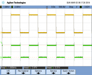
This week, I spent a significant time in the lab and ensured that circuit was able to send the data accurately through the LEDs and that the receiver FPGA when attached to the receiver circuit would read a 0 bit as a 0 and a 1 bit as a 1. In other words, I was trying to ensure that the output from our circuit was high enough to be registered by the FPGA as a 1 when necessary. This involved tweaking parameters for logic levels within the FPGA as well as resistor values and op-amp rail values in the circuit. In order to determine this, a 1kHz square wave was generated using the transmitting FPGA and connected to the IR LED circuit. Connected to that we had our circuit from last week which had the photodiode and amplifier. Next, the receiving FPGA was connected to the output of the receiving side of the circuit and saw the waveform digitally as well as through an oscilloscope. The idea was to replicate the input 1kHz square wave we were sending as accurately as possible. Attached below are some oscilloscope screenshots which show successful transmission and the accuracy.
The yellow wave represents the input wave to the IR LED and the green represents the wave seen at the receiving FPGA. As the graphs suggest, we were quite accurate in the transmission. The difference between the high and low voltages was enough to make them discernable to the FPGA.
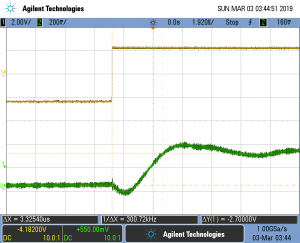
On zooming in, we measured the skew of the transmission (measured to the 90% high mark). We have a skew of about 30us which is very small and expected. This does not affect our design because we had planned for the skew to be slightly larger. Additionally, since we have multiple FPGAs, we know that there is going to be a difference in their clocks which is orders of magnitude higher than this skew. Our design works such that the modulation algorithm and access protocols on the FPGA take care of this skew.
With regard to the second goal of redesigning the circuit, I tweaked some component values so that we get the same output without the inverting amplifier which we had included in last weeks circuit design. This was a significant reduction in circuit components making our circuit more compact than before. This update will be reflected in our design document which is due this Monday.
Finally, we need to order parts for the circuit next week. I have finalized the LEDs for the circuit however, I still have to select the correct op-amp. The key aspect is that the op-amp has to have a high gain-bandwidth product and a high slew rate so that at the frequencies we plan to operate on, the transimpedance amplifier works properly and the skew in amplification does not affect our access protocols. The op-amp still needs to be selected before the parts are ordered sometime next week.
Raziq’s Status Report (Mar 2, 2019)
This past week was the Design Presentation, which I was responsible for. The presentation forced us to condense our thoughts and ideas into concrete specifications and plans, and the feedback received has helped refine our designs in time for the Design Report.
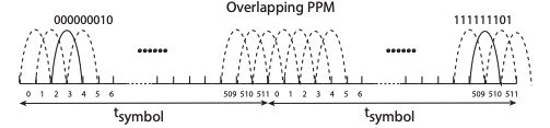
The modulation/demodulation techniques have continued to be a challenge, mostly because there is a wealth of theoretical papers on the subject but a dearth of reliable and affordable implementation details. For our Design Presentation, we had to present the scheme which we had the most concrete information on – Overlapping Pulse Position Modulation, from the DarkLight paper. In short, OPPM is a modified PPM technique where data in encoded in the rise time of pulses within symbol frames.
The number of time slots per symbol frame directly correlates to the number of bits per symbol. The DarkLight authors were limited to a minimum of 800ns as the pulse width, and through experimentation they arrived at a 3.2us slot width and 11 bits per symbol, which leads to a ~6.55ms symbol frame width and 1.6Kbps data rate. We are not beholden to a 0.007% duty cycle limitation, so I’ve still kept options such as OOK in the back of my mind.
In terms of EDC, I have found Verilog implementations of encoder/decoders for codes such as Reed Solomon. I haven’t yet tested with them due to the immediate focus on modulation/demodulation, but I don’t anticipate this taking very long.
Upcoming work
Select the correct Op-Amps.
Order photodiodes, LEDs and OpAmps
Test rise time, gain, bandwidth, etc. for purchased components
Figure out how to use FPGA power for the Op-Amp rails.
Test out modulation/demodulation techniques
Implement clock/data recovery and error detection/correction modules
Implement wrapper modules for Pong to be networked
Team Status Report
As a team we are working on completing the Design Report. We have been incorporating feedback and suggestions from the Design Presentation. We are also identifying parts to purchase for our MVP. We aim to order them before spring break, so that we have sufficient building and debugging time.