Team Status Report for 2026-10-10

This week, we completed our design report and made progress on both software and hardware. In terms of software, we made progress on the emulator, as well as converting bare-mental implementation to using RTOS tasks and an embedded UI. For hardware, we completed the layout and ordered the PCB over fall break.

Our main risk is that the PCB ordering was delayed; however, the order was approved and will ship within the next few days, when we can assemble the PCB in TechSpark; we also planned for fall break and the week after as a buffer in case this happened. We also wrote about global, cultural, and environmental factors below. A was written by Maggie, B was written by Sophia, and C was written by Tucker.


Global Factors

The global factors we considered are tied to some of the main motivations of this product, which is to address the universal concern of technology addiction, internet safety, and healthy digital boundary for especially the younger population. Nowadays, children need to communicate independently and participate in digital activities without unrestricted access to the public internet. We design the product to address this need through a constrained application environment, messaging, and location tracking system to support the children’s independence while helping parents and supervisors monitor their safety and digital boundaries. Besides this, we also want to provide an alternative communication method using LoRa for situations where cellular service is unavailable, unreliable, or unaffordable. For now on the prototype, we use the 915MHz band, and we would adjust this frequency on future versions if we plan to use it in regions outside of the US.

Cultural Factors

Parents must often send their children to school or other spaces, such as after-school activities or playdates, independently. Our product provides a solution for parents to feel more comfortable with their child’s independence through being able to communicate with them while still maintaining safety both virtually and in the real world. The amount of hours that the child spends away from their parent may differ depending on age, family values (e.g. allowing children to play outside until late vs. keeping them at home without explicit permission), extracurricular activities (sports, cram school, or lack thereof), and more; however, we would like the battery life of the product to last 16 hours idle to allow for recharging during 8 hours of sleep.

Environmental Factors

In terms of environmental factors, we primarily considered material use, energy consumption, repairability, and e-waste. For our prototype, we use components such as LCD screen and LiPo battery, which rely on raw materials such as liquid crystals and lithium. Since they are off-the-shelf, we designed the device to reduce unnecessary resource consumption by using a rechargeable battery, and utilized a minimal number of low-power components required for the spec to reduce current draw. We also attempted to make as many aspects of our design modular as possible in order to reduce the need of replacing the entire device when one sub-component requires repair, thus improving the product’s lifespan and reducing e-waste.
Sophia’s Status Report for 2026-10-10

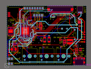
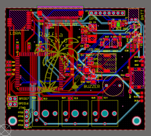
This week, I finalized a first version of the layout for the main PCB. Initially, the plan was to create a PCBA with the ESP32-P4 IC on it; although a layout was created for this version, due to issues sourcing the part, we pivoted to a WT0132P4-A1 module with the flash and power distribution integrated, and assembling the PCBs ourselves. This greatly simplified the layout of the PCB; however, it required us to switch from 3.3V/1.8V to 5V. This meant that instead of having a 1.8V DCDC (which is now integrated into the module), we needed to have a boost to 5V instead, along with keeping the 3.3V LDO for the peripherals. I also modified the LiPo charger to one that allowed the board to switch to USB power whenever it was plugged in, and regulated to a consistent 4.5V or below. This was then boosted to 5V for the processor and regulated to 3.3V in parallel. I also switched the 15V boost IC for the display to a constant current boost.

I was able to order the PCB fabrication along with the stencil on JLCPCB, and am planning to order the rest of the parts this week. When we have all of the parts, we plan to use the reflow oven in TechSpark to assemble our PCB, as there are many surface-mounted components. If the PCB and components do not arrive in time, I will be updating the housing design and working on a hardware testing plan.

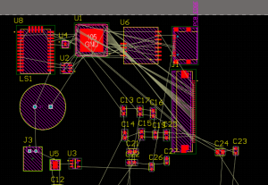
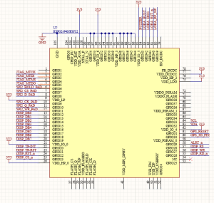
v1 of PCB layout with ESP32
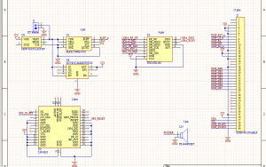
v2 of the PCB layout with WT0132P4-A1

Maggie’s Status Report for 2026-10-10

This week, I’ve been mainly working on drafting the design report. I also placed the GPS module breakout board order, and while waiting of the delivery, I worked on familiarizing myself with FreeRTOS since we need to switch from bare-metal given the increasing software complexity and timing management need.

I read the official docs since we will be using an ESP modified version of vanilla FreeRTOS to learn about configurations and APIs to use it in the Raffia app. The next step would be converting the existing testing functions running in an infinite loop into RTOS tasks.

Besides, I also explored embedded UI approaches. After comparing a couple different framework options such as Embedded Wizard, I decided to go with LGVL given its lightweight and compatibility with Mac since that’s my dev environment. Over the next few weeks, we will continue refining the UI based on the implemented functionalities to make it more intuitive.

The firmware development is still on schedule. Depending on the PCB arrival time, I might need to work on as many scaffolds as possible over the next two weeks to reduce the integration work later.

Tucker’s Status Report for 2026-10-10

This week, I found myself busy with midterms and interviews. Nonetheless, I’m ahead of where I expected on emulation (so far) and working on the design report.

I’ve pulled in Martin Hellspong’s `r68k` CPU emulator as an EC000 stand-in for the time being. I’m not sure if this will be viable for the final integration, as we may have tight margins on CPU performance. However, this allows me to work on emulation and package/IO integration simultaneously, because r68k defines an interface for memory/flash/MMIO and interrupt controller that also works for my version. (Memory, being a hot path, will almost certainly need tighter integration on the integrated board, but I don’t have data to prove that yet.) I’ve also completed further work on my version of the emulator, being able to decode the whole instruction set and execute a subset.

The net result is that we can run the test programs I’ve written, outputting to a MMIO-configured UART. We can also run about 25 million instructions of PalmOS before we hit a yet-to-beimplemented device (one of the GPIO controllers). The challenge right now is mimicing the VZ memory bus: in order to get this far in boot, I have 9 virtual devices (lumping the GPIOs into one, which is not quite true, because they all correspond to different external devices!)

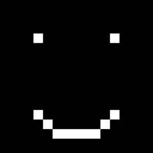
We’re not far enough in boot to draw on the screen yet, so… Here’s a smiley face I drew on the LCD controller! My first drawing in 68k assembly. Brings me back to learning to write code in Small Basic.

A smile drawn in m68k assembly

A fun fact: we’re targeting PalmOS 4.X, which does not do memory management in the traditional sense. It can run 4 groups of memory, and system registers (in the VZ package) are mapped into the top of the address space. PalmOS 6.X was supposed to introduce memory protection, but came only towards the end of Palm’s success. (This is a major factor in why we’re running PalmOS, and not just the apps, since they do not have not a modern expectation of isolated memory.) I wonder if they are the last popular general-purpose computers to lack an MMU, but I have not pursued this line of research.

I’m quite happy with the results this week! Now on my end, the goal is to keep squashing discrepancies with the VZ so we can keep booting. Part of that will be setting up a debugging system so I don’t have to keep flipping between the emulator and my disassembler. The major risk at this point is in emulator speed: I intend to update our schedule with time for benchmarking r68k on our dev board.

Sophia’s Status Report for 2026-10-03

This week, we prepared for the design review presentation, finalizing the design requirements. I also finalized the schematic, adding headers, buttons, boot/reset mechanism, and a 15V boost converter for the LCD backlight.

We decided to switch GPS modules to one that was easier to test with a dev board (from L96-M33 to LC76G), and I added footprints for every component and did a rough layout. Next, I will need to adjust some of the pin orders for ease of layout, align components, and finish routing. I am planning to finish most of the routing by tomorrow night, and order the PCB by Wednesday. I am a little behind schedule, but I have more time tomorrow to spend on this project than I did in the past week.

Team Status Report for 2026-10-03

This week, we completed our design review presentation and have made progress on both software tracks, which is the emulator and instruction decoding and baseline ESP32-P4 firmware development. We’ve also made a preliminary physical enclosure design.

Our most significant schedule risk right now is that we haven’t placed the orders for the PCB, GPS, and LoRa modules. This could delay the PCB bringup and development of the peripheral drivers. Therefore, our immediate next step is to finalize and order all of them at the beginning of next week. Since we have gotten the ESP32-P4 dev board, while waiting for the delivery, we will continue the emulator development and build the firmware scaffolds using placeholder peripherals.

The primary design change happened this week was moving the embedded framework from esp-hal to ESP-IDF. This was a necessary change since esp-hal doesn’t support our MCU’s silicon revision. This change doesn’t affect our hardware choices, system requirements or emulator development but incurred some additional setup and implementation work as it uses different interfaces. However, it was a quick pivot and doesn’t affect our overall timeline or development plan.

Here are some photos of what we worked on this past week:

Maggie’s Status Report for 2026-10-03

We had our design review presentation earlier this week. During the later half of the week, the ESP32-P4 dev board arrived, and I started working on setting up and implementing the firmware framework for the peripherals.

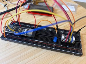
Since we haven’t ordered the LoRa and GPS module yet, I did the development on a ICM20948 IMU as a placeholder. For now, I had a breadboard setup, including the ESP32-P4-WiFi6 dev board, an LED for signalling, and the IMU, connected via jumper wires. The dev board is connected to and powered by a MacBook over USB-C, and it supplies 5V via VBUS to power the LED and the IMU.

I first worked on setting up the toolchain and dependencies for compiling, flashing and running the firmware. Originally, I was planning to use the esp-hal since it’s in Rust and will make the later integration with the Palm emulator easier. However, I found it’s not compatible with our MCU’s silicon revision, since it requires v3.x or newer while we have a v1.x. Therefore, I switched to using the ESP-IDF framework and configured it for the board’s v1.3 chip and 360MHz clock.

Once that was sorted out, I worked on familiarizing myself with the hardware and the framework and then testing several interfaces that will be needed (and could be reused) by the final GPS and LoRa modules. I ran a LED Control test by controlling one of the board’s GPIO pins using PWM with ESP-IDF to achieve a simple pulsing effect. This verifies GPIO and PWM, and we could also later use the LED as a status indicator. 

Then I tested both I2C and SPI by checking the data transmission between the Mac and the IMU. The IMU has 9 DoFs, so for simplicity, I skipped the magnetometer and only tested the accelerometer and gyroscope. I was able to successfully see measurement readings from the IMU every 100ms using the IDF monitor tool.

After that, I tested UART by having the MCU receive inputs from the Mac in the IDF monitor, and the inputs could also be used to control the start and end of IMU readings.

For next week, I will place the GPS and LoRa module breakout board orders and start working on the software for those peripherals. Depending on when they arrive, the goal is to either have correct GPS measurement with parsed latitude, longitude and timestamp outputs or successful message transmission and reception via LoRa. While waiting for the delivery, I will also start preparing the driver interfaces so that I can move on to testing as soon as the hardware arrives to make sure we are still on schedule. Besides that, we will also work on the design report.

Tucker’s Status Report for 2026-10-03

Tucker’s Status Report for 2026-10-03

This week, we had our design presentation and continued forward with our schedule. In the near future, we need to order our PCB and complete our design report.

I spent quite a bit of time getting comfortable with the 68k instruction set this week, and what the PalmOS binary actually looks like. I spent some more time writing assembly in Easy68k. As an aside: it’s fitting that my version of Easy68k requires x86 emulation to run on my Mac.

I also built familiarity with disassembly and binary analysis of PalmOS. My tool of choice is Ghidra, though its 68k support is not as complete as other architectures. In particular, I found that its analysis tools regularly failed to run unless I manually entered function signatures. I identified utility routines including strcpy, a CRC16 routine, an entry point for a built-in debugger, and a lot of IO/MMIO. In reading the binary, I learned that I’d made an incorrect assumption while learning about the architecture: byte and word operations do not clear (or sign-extend) into the full width of registers, matching x86 byte and word registers, but not the x64 doubleword-to-quadword extension that I’ve programmed against more often.

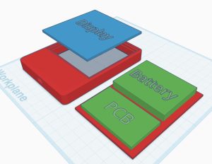
Work on the case will be useful for informing PCB design, and vice versa. I’ve developed an initial model where the display (with flex cable folded under) can be glued into the top of the case, and the mainboard and battery sit on a sled underneath. It helped develop a few constraints:

– The mainboard must go at the bottom of the device to make the buttons at the bottom work. (I’ve omitted the buttons from the screenshot below, because their placement will be defined by PCB constraints, but they’ll be top-hat style 3D prints that rest on the PCB buttons and can’t fall out of the case.)
– Therefore, the battery must go on top. The battery takes up the majority of the internal volume, as well as weight. The combination of display and battery on top is going to be heavy, and we may want to consider intentionally adding weight to the bottom of the case for balance and comfort, potentially at the cost of overrunning our intended weight limit.
– There is enough room for our LoRa antenna to reach around the battery to the top of the assembly. Despite the lower PCB placement, the antenna can be placed such that it won’t be obstructed by the body or left/right hands.
– The GPS IC will likely end up in a position where it may be obstructed by hands during use, since it must go on the PCB. Modulo EMI, testing with a piece of cardboard suggests that it will likely be least obstructed near the USB port, since there’s little reason for fingers to cover that area for extended intervals. I also considered whether we could place it on the back of the PCB, but that risks a prolonged obstruction by the palm of the hand.
– The USB port placement risks conflicting with button placement. However, we could place it off-center or extend the case out further.

Some factors that will depend on PCB design or upcoming team decisions:

– PCB mounting. I’d prefer to place drill holes on the PCB and add either self-tap screws or fully 3D printed pins into standoffs. I’ll have to experiment with pin and clip style attachments, as they seem preferable, largely due to straightforward reusability. However, screws are the simplest on the modeling side (add a ~4mm standoff with solid fill, and tap into it with a short screw).
– Backplane attachment. I modeled it as a plate that glues onto a recessed edge in the case, but this fails to meet our repairability goals. Screws would be difficult to fit around the battery and require more space above the display. We could implement a hinge, sled, or magnetic attachment. I’m slightly enamored by the idea of a hinge, and may prototype it; however, I think that the choice of mechanism is not a priority here, and a sled is a good backup (if potentially annoying to dial in on a 3D printer).
– Display attachment. I modeled it as gluing into the front of the case; this actually performs quite well for repairability, as it could be removed from behind with a heat gun or exacto knife. This is sufficient for a prototype. For a demo device, I’ll prefer to hide the edges of the display under the bezel, for both durability (protect the touch sensor) and appearance.

I made some progress on the emulator and instruction decoding, but no significant milestones here. That was an early goal, and my work on it will continue in the coming week.

Next week: our team is laying out the PCB, writing our design report, and keeping at software. I’ll be focused on emulator milestones this week. I also need to add a time to revisit the case design and do test fits to the schedule – TBD, but this will likely be a week or two after our PCB arrives.


Sophia’s Status Report for 2026-09-26

This week, I was mainly working on finalizing components and creating the schematic for the PCB, along with working on the design review presentation.

We decided on the ESP32-P4 microcontroller for our main architecture. Originally, we were planning to use the eval board (ESP32-P4-WIFI6) mounted on our PCB, but were unable to due to there not being enough GPIO pins. As a result, the schematic has most of the main components (outside of input capacitors, pull-up resistors, etc.) but currently does not have the circuitry for anything that was handled on the eval board itself (such as power management, USB connection, and flash memory, and the clock) as the schematic symbol was changed recently. I am planning to copy these from the recommended hardware documentation as well as the eval board schematic. I also preordered 2 of these microcontrollers on the PCB assembly site I plan to use so that they are available for when I order my PCB.

For the LiPo battery, I decided on an MCP73832 for USB charging, along with a MAX17048 for gauging the battery level. These choices were based on Adafruit’s dedicated boards for these tasks; however, to save costs and space, I decided to put the ICs on my board directly. I also decided on a NCV8187 3.3V LDO regulator to supply power to the rest of the board, since the difference between the voltage of the LiPo battery is relatively small for most of the time, making the efficiency comparable to a buck converter.

I also selected connectors for the screen and battery, as well as a passive buzzer. I am slightly behind schedule, since I have not fully finished my schematic; however, I have selected all key components, so most of the work lies in creating the remaining components in my design software and double checking datasheets. This should not be a large issue, as the week I have allocated to ordering the PCB also doubles as buffer time. Next week, I need to work on layout, as well as the design report.

Maggie’s Status Report for 2026-09-26

This week, I was mainly working on the system design and architecture of how the major processing, communication, display, and power subsystems interact with each other. This includes the esp32p4 MCU, GPS and LoRa modules, touchscreen, battery charging and protection, voltage regulation, and thermal monitoring. I then worked on creating the system block diagrams and preparing the corresponding design slides.

I also worked on comparing our processor and peripheral options and helped finalize the specific modules we would like to proceed with, with a main focus on their processing power, power needs, development support, and compatibility. After finalizing these decisions, I have started working on developing the GPS firmware.

My work is currently on schedule overall, although the hardware selection phase took a bit longer than initially expected because we reconsidered a few different processor architectures. The main processor (and the corresponding dev board) and initial peripherals have been finalized now, so we have a stable architecture that we can start developing on.

I’m currently working on developing and testing the GPS and LoRa interfaces. This will be done on the dev board while the custom PCB is still being designed. In terms of GPS, the goal is to complete a minimal version that reliably reports latitude, longitude, fix status, and timestamps before we start adding more complicated configuration and power management features.

Next week, I plan to complete the first functional version of the GPS interface (specifically the driver configuration and message NMEA message parsing) and begin LoRa message transmission, and the expected deliverables will be committed GPS code and potentially an updated system diagram and LoRa bring-up code.