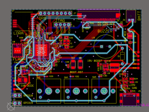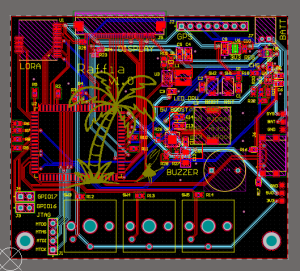
This week, I finalized a first version of the layout for the main PCB. Initially, the plan was to create a PCBA with the ESP32-P4 IC on it; although a layout was created for this version, due to issues sourcing the part, we pivoted to a WT0132P4-A1 module with the flash and power distribution integrated, and assembling the PCBs ourselves. This greatly simplified the layout of the PCB; however, it required us to switch from 3.3V/1.8V to 5V. This meant that instead of having a 1.8V DCDC (which is now integrated into the module), we needed to have a boost to 5V instead, along with keeping the 3.3V LDO for the peripherals. I also modified the LiPo charger to one that allowed the board to switch to USB power whenever it was plugged in, and regulated to a consistent 4.5V or below. This was then boosted to 5V for the processor and regulated to 3.3V in parallel. I also switched the 15V boost IC for the display to a constant current boost.
I was able to order the PCB fabrication along with the stencil on JLCPCB, and am planning to order the rest of the parts this week. When we have all of the parts, we plan to use the reflow oven in TechSpark to assemble our PCB, as there are many surface-mounted components. If the PCB and components do not arrive in time, I will be updating the housing design and working on a hardware testing plan.