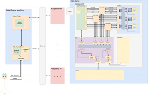
Accomplished Tasks:
- Designed Top-Level Block Diagram
- Wrote Transport Layer Protocol
- Made FSM Diagrams for Model Manager, FPU Bank/Job Manager, and Memory Management Unit
- Setup barebones benchmarking suite for local machine CPU
Risks
The most significant risk is that we don’t get connectivity working between the Data Source machine and the synthesized hardware. Our contingency plan is to implement the easiest solution possible, which involves having a Raspberry Pi act as a network stack for the FPGA and transmitting data to the board via GPIO. This mitigates the risk because implementing a GPIO protocol in hardware will be much easier than implementing an Ethernet network stack in synthesizable hardware.
Another big risk is that our bus cannot handle the desired throughput and the worker boards spend significant time idling.
Changes Made
We decided that, instead of implementing an Ethernet network stack in Verilog, we would use a Raspberry Pi to handle the internet protocol and communicate information from the Data Source server to the Worker board. This means it will require a lot less work to implement functional connectivity between nodes in the network. This change incurs the cost of a single Raspberry Pi board for each worker, which brings the effective price of a Worker from $89 to $134, which is still within budget for the number of Workers we plan to buy.
Schedule Changes
We spent this week producing design documents to aid our process going forward. We have also realized that the development of hardware components will require more effort than anticipated.
Theodor (TJ) will spend the next few days finishing all of the documentation for the hardware side, excluding the GPIO protocol (still to be implemented by Jared Rodriguez). He will spend the rest of the next week putting together memory interfaces for the M9K Blocks and off-chip SDRAM, some of which can be recycled from his work in 18-341.
