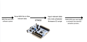
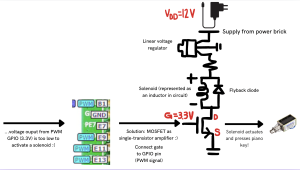
This week, my primary focus was on preparing for the design review presentation. As part of this effort, I created the hardware system block diagram, which outlines how the different components of our project will interact with one another- find attached below. Additionally, I worked on designing the electrical circuit (visible in the second image) for the solenoid control system. This design includes obvious components, but I’ve realized that integrating MOSFET amplifiers is critical to making the circuit function properly. This is because the signal output by the GPIO pin is 3.3V which is too low of a voltage to input into solenoids + activate them. Hence, a common source NMOS configuration can amplify.


Unfortunately, I fell slightly behind schedule this week due to two midterms and the preparation required for the design presentation. I wasn’t able to begin running the Cadence simulations, as planned, but I will prioritize this first thing next week. To catch up, I’ve already blocked out additional time to focus on running these simulations and ensure the electrical circuit I designed operates as expected.
Next week, I plan to finalize and run the simulations in Cadence, ensuring the circuit is functioning as intended. Additionally, I will focus on learning more about how Pulse Width Modulation (PWM) works and how it can be integrated into our system to improve power efficiency. I’ll be working with Peter to begin testing how one solenoid works.
