Xiran’s Status Report for 10/2

This week, I transitioned from working on the communication portion of our project to working on the DUT. Namely, I finalized our ISA and designed the datapath for our DUT.

Designing the ISA involved several decisions: deciding 1) the number of bits, 2) the instruction format, and 3) the instructions themselves. For 1), I settled on 16 bits because it allows us to lesson the communication cost of the system, while still keeping the number large enough that it doesn’t become a toy example. For 2), I used the simplest scheme I could think of in the interest of making our instruction decoder simple, as is typical in a RISC architecture. For 3), I examined ISAs I have studied (x86, ARM, RISC-V) and chose 16 arithmetic/logical instructions that are in most ISAs, as these are the crucial ones.
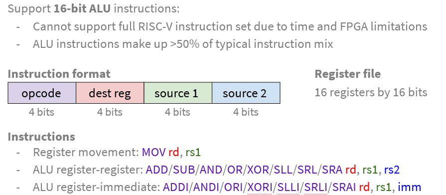
Summary of our ISA

I also designed the datapath for our DUT: a single-cycle microarchitecture implementing this ISA. There aren’t many design decisions involved here. I simply chose the most simple datapath with my computer architecture knowledge.

DUT datapath block diagram

In addition to these individual tasks, I also worked on benchmarking simulation speed and the design review slides.

It should be noted that my action items did change this week from what I had planned. I originally planned to start working on the golden model this week, but given that it would be nice to have a concrete diagram of the DUT for the design review, I prefeteched the task of designing the datapath. However, I am still on track to meeting my deliverables. Next week, I will work on and finish the golden model.
Team Status Report for 10/2

The most significant risk that could jeopardize the success of the project is still in the communication protocol. Last Sunday, we made the decision to use Ethernet for communication. This week, while waiting for the Ethernet cable to arrive, Grace and Ali prepped by spending considerable time researching the protocol, including how the 88E1111 Marvell PHY Chip is connected to the board and its Ethernet ports. Next week, Grace and Ali will implement the protocol. We also plan to try out USB demos in the case of running into unresolvable issues with Ethernet.

The risk of the design not fitting on the board is also being managed. The finalized DUT ISA is intentionally small to mitigate this risk. In addition, we are looking into how much space the NIOS II processor takes up on the FPGA, so we can get a concrete number of how much is left for the DUT.

As for changes to our project, we worked on strengthening our project motivation and the requirements based on Proposal Presentation feedback. Instead of motivating solely with runtime gains, we will also highlight, in the future, how the FPGA approach allows the design to be tested in actual silicon instead of only in software. We also added a requirement of being able to support test cases of size 1 ~ 20k instructions, as a quantitative measure of what we can support was missing in the Proposal.

We do note that some of Grace’s and Ali’s work with Ethernet have been delayed due to waiting for equipment, but work will pick up next week. We may update the schedule next week depending on progress, but at the present, there are no changes.

Ali’s Status Report for 10/2

This week I worked with Grace to learn more about the Ethernet ports on the FPGAs. Initially, we planned to run through the last demo that came with the DE2-115 boards (the demos can be found in the user manual – chapter 6). Because we were waiting for a USB-USB cable and a dual ended ethernet cable to come, we did not have the chance to run the demo. I am planning on running the demo later today or tomorrow. We were hoping to see a little bit more about what exactly using the ethernet port looks like in reality.

Because we were waiting to receive the cables, I spent most of Monday/Tuesday trying to look for resources on ethernet on our FPGA. Grace found information about the NIOS II processor which is a processor that runs on the FPGA’s internal components and makes it easier for users to interact with the components on the FPGA. I found this tutorial on creating a processor with the Triple Speed Ethernet ports (TSN Ethernet). I started walking through the tutorial on Wednesday to try to understand more about the process, but again, I couldn’t test it with the board because we received the cables on Thursday or Friday. A lot of my time this week was spent trying to find more resources on the TSN Ethernet ports, but there don’t seem to be too many resources. However, I did find the manual for the ethernet ports.

Lastly, I spent time research projects people have developed using the TSN ethernet and I tried to find some github projects with TSN ethernet, but I could only find people’s documentation not github repos. Most of our progress was hindered because we had to wait for our cables to come.

I also worked with Grace and Xiran to run tests on simulation to have a better idea of how long it takes to run some of these tests. I think we are a little behind where we wanted to be — I was hoping we would have been able to run some tests on the FPGA, but I am confident that we’ll be able to implement the ethernet protocol. Grace and I are probably going to meet Monday afternoon and work on the protocols some more. We are planning on looking through some of the code for the NIOS II processor to try to understand more about how the processor works, and how to correctly interface with the ethernet ports.

Grace’s Status Report for 10/2

This week Ali and I focused on researching and testing different communication methods on the FPGA. We are already familiar with JTAG protocol methods, so we decided to focus on USB and Ethernet. I found that there are a bunch of demos already made specifically for the DE2-115 FPGA board that we will be using that implement different features of the board. One such test utilizes USB while another uses Ethernet. We were not able to actually run these demos together this week since we were waiting for the right cables to be ordered by the department. The demos are in chapter 6 in the manual (https://www.intel.com/content/dam/www/programmable/us/en/portal/dsn/42/doc-us-dsnbk-42-1404062209-de2-115-user-manual.pdf).

We also investigated how to use the triple speed Ethernet on the DE2-115 boards. I found that we will need to instantiate the NIOS II (a softcore microprocessor) on the board (using LUTs), which will connect to the 88E1111 Marvell PHY Chip on the board. I started looking through the documentation and short usage video chips on the NIOS II processor using their developer support tools (https://www.intel.com/content/www/us/en/programmable/documentation/lro1419794938488.html#mwh1416946569962). Unless we are willing to buy the license for the others, we will need to use the lowest performance NIOS II processor (version NIOS II/e).

I also worked a lot on the design slides for the next week’s presentations and did some practice runs as I will be the presenter for our group.

Additionally, our entire group worked together to determine which speeds we will need to meet for our project to meet its performance requirements. We ran some simulation tests and determined that we will need to use gigabit ethernet to achieve the necessary speeds.

Next week, Ali and I plan to run some of the demos and look through the code in the demos to see how they configure the NIOS II processor.

Grace’s Status Report for 9/25

This week I focused on researching different communication protocols to be used for communicating between the PC and the FPGA board. I mainly researched Ethernet methods, but also looked at some USB ideas from my teammates. By comparing other thesis or final design projects from other universities, I found that there are methods for performing the tasks we need, but while Ethernet is very fast for performance metrics (can support 10Mbps, 100Mbps, and 1000Mbps), it is very difficult to implement in the DE2-115 Altera boards we are using (https://etd.ohiolink.edu/apexprod/rws_etd/send_file/send?accession=dayton1448287709&disposition=inline).
I discovered that one of the more challenging aspects of creating these protocols on this board is correctly using the NIOS II soft microprocessor. Both Xiran and I have embedded experience, so I am hopeful that by digging through the handbook for the NIOS II we will be able to effectively use it (https://www.intel.com/content/www/us/en/programmable/documentation/lro1419794938488.html#mwh1416946569962). We are also planning on reaching out to Bill Nace to see if he has any experience with NIOS II on these specific boards.
This upcoming week we want to test different protocols (if possible) using basic “ping” style tests. I found that the DE2-115 boards have demos in their manual kits that use both USB and Ethernet protocols. We are hoping to try to use those this week to learn how the built in tools work. I am currently on schedule for my deliverables. We are planning on meeting this week as a team to decide which method to use in our project.

Ali’s Status Report for 9/25

I spent this week focusing on 2 things:  preparing for the proposal presentation, and also researching the JTAG protocol. I spent a decent amount of time making sure that I was ready to present and could have a decent presentation.

Next, I spent time trying to understand more about the I/O protocols that the DE2-115 FPGA can manage. I found the user manual and started investigating how to debug JTAG vs USB vs Ethernet. It seems like JTAG has some of the expected benefits and detriments — easy to use, but might not be fast enough. Typically, JTAG can transfer data at a rate between 10 MHz and 100 MHz. Although this might be fast enough to send data in 1 direction, it might not be able to support sending enough data from the FPGA to the PC.

I think I am a little behind schedule, but I am planning on finishing up research and playing around with an FPGA early this week, and then working with Grace to develop the communication protocol.

For next week, I’m hoping to have finished or nearly finished the FPGA protocol.

Team Status Report for 9/25

The biggest risk for our project remains to be the communication latency between the FPGA and the computer. This week, each of us researched one of three communication protocols under consideration (JTAG, USB, Ethernet). Tomorrow, we will meet to discuss choosing a protocol. Work on implementing the protocol will begin next week.

Another point of concern brought up during our Proposal Presentation is whether the size of our DUT will fit onto the FPGA. Work on designing the DUT ISA will also begin next week, and taking into account this feedback, we are considering limiting the design to an ALU. This will allow us to mitigate this risk.

There have been no changes to the requirements or the schedule.

Xiran’s Status Report for 9/25

I spent this week researching FPGA communication protocols. I was assigned USB, so I started with that. I found the following key pieces of information from the DE2-115 User Manual:

  • The board provides a USB device interface, supporting data transfer at 12 Mbit/s
  • There’s a demo with complete driver code that connects the board to a host PC and allows the PC to control some components on the board (such as LEDs)

I dug for user-side information on this topic too (e.g., customized driver code) but was not able to find much. This lack of information makes the usability of USB concerning to me, so I also looked into Ethernet. Surprisingly, I was able to find an open-source Cornell project that implemented Ethernet communication to the board. This may be something we can use off the shelf.

I am on schedule for my deliverables. Next week, I will transition to designing the ISA for our DUT. My thoughts so far are to limit the design to an ALU that supports common arithmetic and logical instructions, but details (instruction format, number of registers, etc.) need to be worked out. By the end of next week, I plan to have the complete ISA and to have begun working on the software golden model that implements this ISA.

Team Status Report for 9/18

For our project, the most important design requirement is the runtime for completing tests. This runtime will consist of three components: the time it takes to send test cases to the FPGA, to actually process the tests through the DUT, and to send results back from the FPGA. Given that the FPGA runs on a fast hardware clock, we don’t expect the second component to take long. Instead, our bottleneck (and our biggest risk) will be in the communication latency to and from the FPGA.

For the next few weeks, we plan to focus our efforts on managing this risk. We will research different communication protocols available to us, pick some to implement, then pick one that meets our requirements through benchmarking.

Grace’s Status Report for 9/18

This week I focused on helping our team finalize our project idea. We came into the week bouncing a few more ideas around until our meeting with Tamal and Joel. Based off of their suggestions, we decided to focus on the general idea of using FPGA prototyping to speedup simulation. Using our experiences in 18-447, we decided to focus on a debugging assistance tool that can compare the output of the DUT on the FPGA with a software golden model cycle-by-cycle. We realized that our most important design decision would be deciding how we communicated with the DUT to feed it input and receive the output. As such, I researched and conferred with my teammates on different methods of sending data.

To gain some more advice, we met with Professor Bill Nace to discuss the attributes of the Altera FPGA boards available in the lab. Based off of his guidence, this upcoming week will have us focus on testing different communication systems (usb, ethernet, etc.) with the FPGA. We are hoping that by the end of the next few weeks, we have modeled an efficient method of sending input and receiving output.