- Work this week
- This week I debugged several more issues with our PCB. I continued work on the comparator issue. I tested our two new comparators, but they did not work. In fact, they worked worse. I discovered several things. One is that the comparator overdrive ranges are all specced far better than reality. The other is that this was not the actual issue. The real problem is that our charge pumps create a huge amount of noise. They do not create noise on their outputs. However, the radiated emissions from them induces current in the traces to the photodiodes. Because we measure current on order of magnitude of microamps, this noise is far greater than our signal. To fix this, the charge pumps should be far away from receivers, with long traces carrying the reference voltage over. However, this cannot be fixed without a new board spin. In the end, I fixed this by only using only the green photodiode photodiode, and the charge pump for the IR photodiode plus a voltage divider to get the correct reference voltage. The reason for only using green is explained in the next bullet. Because the photodiode only draws microamps, a voltage divider creates a sufficiently stable voltage. Because the charge pump is far away on the board, it does not radiate emissions into the signal line.
- I discovered that our infrared laser will not work. The laser only creates a 1 mV signal when turned on directly in front of the receiver. I figure that the receiver’s datasheet showing the optical wavelength response is likely inaccurate, since it shows a graph of a full spectrum, and it is unlikely the manufacturer was able to actually measure this, and we are using a laser below the peak wavelength of the photodiode. This is not fixable without redesign or buying a large number more parts to find compatible ones. This, combined with the aforementioned charge pump issue, led me to make the call to remove IR. The green laser functions, and we do not have the budget or time to fix IR, since the components are incompatible.
- I found a solution to our USB power problem. I got usb power/data splitters designed for raspberry pis and modified them for our use. They allow us to combine a 9V3A usb pd supply and a usb 2.0 data wire into a single usb C wire. I made 2 of these boards and verified that both power and data work.
- I spend a lot of time finding correct resistor values to change precise settings and thresholds for both boards. The current state is that both use green lasers set to 5 mW, and both green receivers are set to correct thresholds.
- I 3d printed and tested our lens mounts. They fit and the lenses allow us to focus the lasers. Additionally, since I included the threaded metal piece, the mounts allow us to focus and unfocus the lasers on the fly. This was done by using a belt sander to file them down to be small enough to fit on the board over both lasers and with good focus.
- I ran a quick test with Anju to see if the laser and fpga work together. They do! On the first try, we were able to send data at 6.25 Mbaud using the laser and receiver. This bodes well for us, particularly since this was done with me holding a mirror by hand in front of the laser, making for a bad signal.
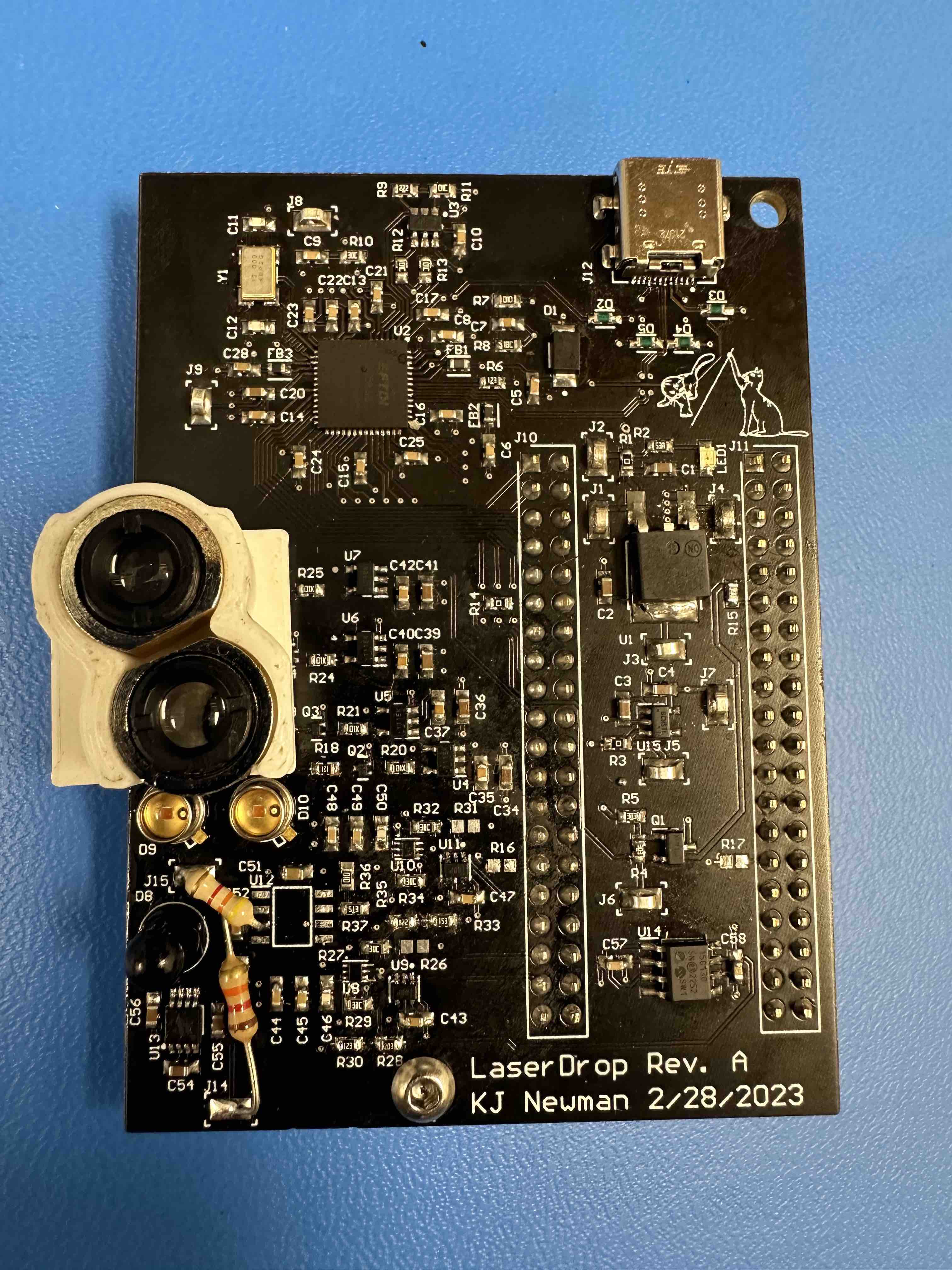
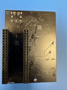
- Image of board now:
- Schedule
- Integration is still behind schedule. Now that hardware seems to be done, this is my number one priority. Since the preliminary test with Anju worked well, and Roger is able to communicate over USB, this seems mostly done. However, we cannot be sure bugs do not remain.
- Deliverables
- Next week, I will finish our second 3d printed housing test. I finished the housing, but I have not assembled and tested it. I also need to use the belt sander to cut the metal pieces down to size.
Anju Ito’s Status Report for 3/25/2023
- Work This Week
- Designed, programmed, and compiled the FPGA FSM and datapath, though it needs much debugging work.
- Got the simulation to run and wrote a testbench. The testbench did not work for a while due to syntax issues with ternary operations, but runs now and there are issues to debug.
- Helped look at EEPROM programming to set the chip to 245 asynchronous FIFO mode using 9V 3A power delivery.
- Schedule
- The code is slightly behind schedule, and I hope to finish debugging the FSM through simulation by this week so that integration goes smoothly by the end of this week or next week.
- By the interim demo, I hope to have a working FPGA code written. Although this cannot be demoed unless an FTDI chip and computer software is written. The basic sending data and receiving may be demonstrated as MVP.
- Next Week
- Finish debugging the full FPGA code through simulation.
- Help out in other tasks as necessary, and possibly integrate with code/FTDI chip/lasers.
Team Status Report for 3/25/2023
- Risks
- This week we fixed several risks, including low laser power and the FTDI power chip not working. However, we also added several more:
- One is that Macs do not support our usb power plan. We need to find a new power solution. We plan on researching available usb splitters and powered usb hubs that may fit our needs. Worst case, we can either hand splice a wire to separate power and data or we can use a power supply separate from USB. However, we plan on looking into better alternatives than that.
- Another risk is that the comparators do not work. Our original comparators for our receivers do not work as well as the datasheet suggests, and therefore our circuit does not create enough overdrive voltage for them to have digital outputs. To mitigate this, we purchased 2 different new comparator chip models that should perform better. They are the same footprint and will work perfectly if the datasheets are correct. If they both end up not working, we can wire in a breadboard with more analog circuits to fix this. However, that would greatly limit our max communication speed, so we are trying new comparators first.
- Simulation on the FPGA had difficulties running due to subtle syntax differences. The biggest of these were debugged, but the ability to easily verify it might be time-consuming in the future.
- Design Changes
- We will need some new part to fix our usb power delivery issue. This is not yet determined, but will likely be something between our board and the laptop.
- We changed how we will be 3d printing the lens housing. Rather than 3d printing threads or a hole for self tapping, we will cut the metal housing we have down to a small size since it has threads that fit our lens already. Then, we just need to 3d print a circular hole for the housing to sit in, which requires much less precise work.
- We plan on removing the sequence tag ID, once we verify that all of the packets can be performed in-time synchronously. This will be dependent on the speed that the computer can read data off the FTDI, verify the Hamming code, and send data back.
- Updated Schedule
- The actual 3d print and assembly of our lens housing has been pushed to next week due to issues with the board that came up this week.
- Board testing continues to be extended as we encounter unexpected issues with the boards.
- FPGA testing will continue on next week, waiting for software and hardware to work before integration.
- Progress
- The board powered over 9V USB PD by configuring the EEPROM connected to the FTDI chip:
- Currently debugging, but a full FSM and datapath for the FPGA was designed and programmed.
- Higher power laser output was produced that can be read better by receivers.
- The board powered over 9V USB PD by configuring the EEPROM connected to the FTDI chip:
Anju Ito’s Status Report for 3/18/2023
- Work This Week
- Began to write FPGA code. Progress:
- Wrote a laser transmitter module that will transmit 2 input data over 2 lasers if the data valid signal is set. This module will always transmit both data simultaneously. This is the desired behavior for the project, as our MVP will never use one laser and not the other.
- Wrote a laser receiver module that always listens for a byte that follows UART protocol (start bit and stop bit). This module was configured so it can only receive both at the same time, and currently making different versions to test the receiver.
- Debugged the laser transmitter and receiver by setting up the waveform viewer environment. This took some time, as the vcs compiler kept exiting on failure. It turns out that the source bashrc has to be called every time, and I have to make sure that I only have setup447 (or one of the class) and not the other, as those conflict with each other now.
- Wrote an untested version of the FSM and protocol handler of the transmitter module.
- Verified functionality of the transmitter and receiver modules by sending constant bytes from the transmitter to receiver using a single board, connected by jumper cables from the laser out line to the laser in line. Successfully sent bit, flashing the data received every time, and allowing for switches.
- Imported pin configurations and assigned appropriate ones based on schematic. Modified code so that all GPIO pins except for transmitting and outputs are high impedance, and labeled/used each one for its set purpose.
- Flashed the code successfully onto FPGA non-volatile memory. This involved emailing/creating a Terasic account to get their programmer, and converting file formats. This makes it much easier to just turn on the device without needing to reconfigure the board every time.
- Integrated the FPGA with the PCB. Fixed issues with DNP resistor labelling that caused the FPGA to be turned partially on (3V3 was connected instead of the 5V to the FPGA. Fixed by removing and putting on the resistors). Verified that the lasers can be somewhat controlled by the FPGA, although there is no way to test it so far as the receiver did not work with preliminary testing using mirrors.
- Began to write FPGA code. Progress:
- Schedule
- Things are on schedule. Since boards have arrived and KJ has assembled them, my implementation from now will most on likely work in parallel with testing the board features and making sure that they will work. This will involve modifying the code and making a simplified version of it which would take some time, but also ensure that the code will work well with the board.
- In addition, since there are potential issues with the receiver and we need to verify the functionality of the lasers, etc. I will use some time attempting to write test code and debugging that feature, which may slow down me working on FSM.
- Next Week
- Write out the full program for FPGA including the receiver FSM, and testing the transmitter FSM. Integrate it with the board and see how far I get.
- Test out the laser transmitter/receiver on the PCB, because integrating with the FPGA may be the easiest way to test the board functionality, since it receives high speed transmission. Since it didn’t register the first time transmitting at 6.25 MHz using a mirror, potential things to do are slowing down this transmission speed greatly, using 2 boards for better laser power going to the other board, turning off ambient noise cancellation, and testing in a dark room.
![]()
Bits being transmitted and received by the receiver module (displayed on the HEX values, the first 2 for the IR receivers and the second 2 for the green receivers). The GPIO pins are connected with jumper cables.
Team Status Report for 3/18/2023
- Risks
- The IR receiver on one board appears to be floating. This is not a huge risk because it is likely a poorly soldered part, but there is a risk that there is something big wrong. We will be looking into this next week to determine exactly what is wrong.
- We tried to do a quick test of the receiver, which did not work. This is most likely due to poor setup, but it may require figuring out how the ambient light filtering works, and how best to aim the boards to each other in order to test accurately, which may take some time and work.
- Design Changes
- Our USB connector did not fit properly on our board, so we needed to bend pins and not attach all pins in order to get it connected. This ultimately resulted in some power and ground pins not being connected as planned. This is not expected to cause any issues but does mean that our board supports less current going through the connector now.
- When writing the FPGA program, we’re slightly split on whether to make it so that both lasers must receive at the same time and transmit at the same time. If we do this, it would add integrity because there is a much smaller likelihood that both would turn on accidentally at the same time, and make handling the protocol easier. However, it would also make it so that testing is difficult. Right now, the decision is that it will only handle simultaneous receiving/transmission, and the code will be modified slightly so that testing can be done with just one.
- Updated Schedule
- We did not do any 3d printing this week due to the assembly process taking longer than expected. This will now happen next week.
- The implementation of the FPGA got slightly overlapped with board integration, and some of the code development would be shifted to testing using the actual PCB.
- Progress
- Boards complete!
- FPGA code written and tested for the laser and receiver module. The FSM that handles the actual protocol behavior is written on the receiver side, but not yet tested.
- FPGA and board integrated, and ensured that GPIO pins control the appropriate circuitry.
- Boards complete!
KJ Newman’s Status Report for 3/18/2023
- Work this week
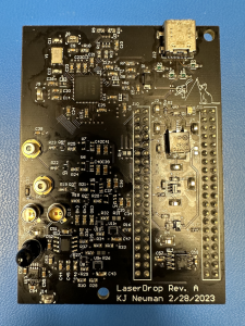
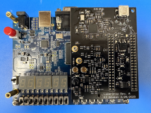
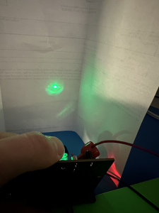
- This week, I assembled two of our PCBs. We did not receive a stencil from JLCPCB, so this took quite a while. The boards assembled as expected with only one exception, the USB connector. The connector requires a board cutout underneath it and the board does not have one, so it took a lot of time to get the connector to fit. Ultimately, I figured out a way to bend the pins and use hot air soldering to get the connector on, but destroyed our 2 other connectors in the process. However, it did work on one board, so we ordered some more connectors to put on the second PCB using the same process. This ultimately will not slow us down much or cost much. The board is shown here:
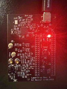
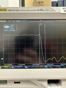
- I also tested the PCBs. The transmission and power circuits work as expected, and the receiver circuits are difficult to test without FPGA software, so I began working with Anju on integrating the FPGA board and the custom board. Transmitting works integrated with the FPGA, and receiving testing is ongoing. All voltages on the board are correct, and laser driving at two different power levels works with sufficient rise and fall time to transmit at our speeds as shown:
- I verified how the lenses fit over our board and that they properly focus both lasers. I also found that iPhone cameras can indeed see our IR laser, but not very well
- I ordered some additional parts this week. I ordered and received 3d printer filament. I also ordered new usb connectors as we ran out.
- This week, I assembled two of our PCBs. We did not receive a stencil from JLCPCB, so this took quite a while. The boards assembled as expected with only one exception, the USB connector. The connector requires a board cutout underneath it and the board does not have one, so it took a lot of time to get the connector to fit. Ultimately, I figured out a way to bend the pins and use hot air soldering to get the connector on, but destroyed our 2 other connectors in the process. However, it did work on one board, so we ordered some more connectors to put on the second PCB using the same process. This ultimately will not slow us down much or cost much. The board is shown here:
- Schedule
- My work is mostly on schedule. I managed to assemble and test pcbs despite not having the stencil. However, this meant that 3d printing our housing fell behind schedule, and I now plan on doing this next week.
- Deliverables
- For next week, I plan to design our 3d printed housing for the lenses and print it. I also plan on continuing integration of the receiver with Anju and giving a board to Roger for him to integrate USB code and EEPROM settings onto.
Anju Ito’s Status Report for 3/11/2023
- Work This Week
- Significant amount of time was spent working on the design report this week, including FPGA implementations, diagrams, and overall project information.
- Began coding modules for clock dividers that will be needed to time UART communication on the USB transceiver and laser side.
- Came up with block diagram for the transceiver, consisting of 2 shift registers that will be enabled depending on number of bits that go into each.
- Schedule
- Design report took more amount of time than originally thought. Implementation will need to be worked on, which will hopefully be done the week after spring break.
- Next Week
- Have an overall implementation of all aspects of the FPGA, so that debugging can be conducted the week after using oscilloscopes for signal accuracy
Team Status Report for 3/11/2023
- Risks
- With the complete PCB design, we removed some of the planned backup plans since they were not feasible. The big one is that we were planning on leaving some extra DNP pads for more green photodiodes in case our photodiodes are not strong enough. However, there is slightly more risk now since we had to remove this to make layout work.
- We noticed that the FPGA board lists some pins as clock pins. The Datasheet does not describe what this means. This is 2 pins from the FTDI chip and the 2 IR laser controlling pins. If this ends up being an issue, we can accommodate it by using an interface with the FTDI chip that does not use those pins (fast serial) and by testing that the IR laser pins operate at high enough speed.
- Design Changes
- Our PCB will be much smaller than the FPGA board rather than a copy of it. This is because the parts fit on a much smaller footprint, and making it smaller makes buttons and LEDs on the FPGA board accessible, and it will be easier to make sure the boards fit together.
- Updated Schedule
- In terms of schedule, software developments (Roger) were impacted by inability to develop software for hardware that had not been fully finalized. We have instead begun working on sender implementation as well as a preliminary UI interface to input text files for sending in order to be productive within the schedule constraints.
- No changes have been made to the hardware schedule as the PCB and part orders went out on time
- Progress
- PCB design is complete! Our PCB and all components for it have been ordered and should arrive by the time we return from spring break.
- Sender implementation for the bitwise hamming encoding of files has been implemented
- We completed our design report paper
- PCB design is complete! Our PCB and all components for it have been ordered and should arrive by the time we return from spring break.
- New Tools
- We will need to learn to use FT_PROG to program the EEPROM to save settings for our FTDI chip
- We will need to experimentally identify the best way to view the infrared laser for debugging and testing. We currently plan on using the front-facing camera from our phones, as they typically do not have IR-cut filters. However, this may not work. In that case, we will need to learn to use an IR camera to measure it.

KJ Newman’s Status Report for 3/11/2023
- Work this week
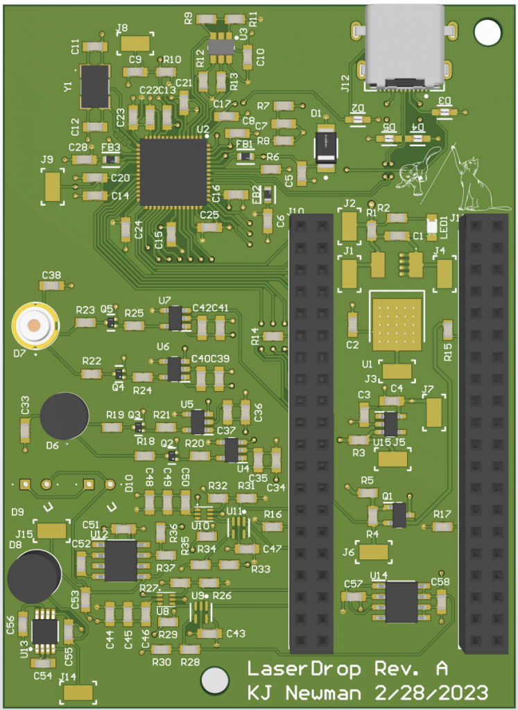
- This week, I completed our PCB design. I did our layout and it passed all DFM checks. It is currently in fabrication at JLCPCB and expected to arrive before class resumes after winter break.
- I ordered all parts to make our PCB. Our only expected expense that has not been purchased yet is 3d printer filament. This has 1 day shipping so can be purchased later. Setting up our part orders was a bit complex because I wanted to order with bulk discounts where possible and buy extra components in case we need them, but we are running a little close to the $600 budget. I ultimately ordered enough active components for 3 boards and numbers of resistors and capacitors to get bulk discounts.
- I wrote my parts of the design report. This was a lot of work to do in parallel with finishing and ordering the PCB, but we managed to finish it.
- This week, I completed our PCB design. I did our layout and it passed all DFM checks. It is currently in fabrication at JLCPCB and expected to arrive before class resumes after winter break.
- Schedule
- My parts are on schedule. I planned on having the pcb ordered before spring break and set to arrive after spring break, and it should be here by then.
- Deliverables
- For next week, I plan to have 2 PCBs fully assembled and ready for use. This should be achievable, since all of our parts will have arrived before the beginning of the week.
Roger Lacson’s Status Report for 2/25/2023
- Personal Accomplishments
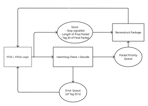
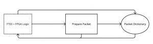
- I have ironed out the algorithm that will be used for both the sender and the receiver software. A block diagram is shown below. I try to minimize information sent and stored to create an efficient algorithm to send and process transmitted data.
- I was recently tasked with Hamming encoding/decoding in software as well as EEPROM configuration. I have begun looking up examples online of how to organize and implement these tasks and have begun writing non-hardware-dependent algorithms. I have also continued understanding COM connections and implementing a VCP and have reached out to friends with more experience in the area on how to implement these ideas. I plan to meet with my friends Wednesday night to better grasp the concepts I have gathered and implement all of these tasks.
- I have ironed out the algorithm that will be used for both the sender and the receiver software. A block diagram is shown below. I try to minimize information sent and stored to create an efficient algorithm to send and process transmitted data.
- Schedule
- My work is on schedule. While I wasn’t able to write pseudocode (again), more of the protocol was ironed out and I have made progress on all fronts regarding my software implementation. Remaining flexible towards hardware changes has been a large focus for me, and I have tried to remain productive while the hardware portion of the project is developed. I believe we are still set up to integrate software, hardware, and FPGA shortly following break, and I plan to implement more code during break to make up for any slack produced at this time while design elements are being finalized.
- Deliverables for next week
- I will meet with my friends to have a better understanding of the code I wish to implement regarding hardware connection.
- Finishing the status report will take priority for most of the week, but I still hope to make progress in my software implementation and have a solid plan going into the break of what needs to be complete.