Anju Ito’s Status Report for 4/22/2023

  • Work this week
    • Finalize laser transmitter/receiver and FTDI interface
      • All inputs go through 2 flip flops to avoid metastability
      • Better timing for all I/O devices
    • Implement handshaking
      • Handshaking occurs before every packet send now
      • Series of 0xAA sent by transmitter. Receiver responds with 0x10
    • Implement packet sending/receiving
      • Sender: send bytes in 1kB chunks. Handshakes before each one.
      • Receiver: receives bytes. If receive < 128kB after handshaking, will pad out the bits with all 1’s
    • Use 128kB buffer on receiver/transmitter
      • If more than 1kB sent/received, FPGA has capability to store that.
      • Created to accommodate for slow USB transmission.
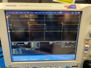
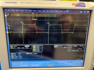
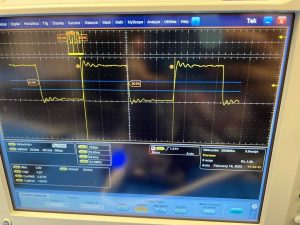
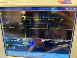
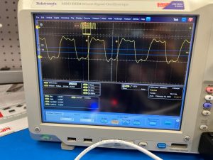
    • Create Manchester/Duty-cycle like encoding for FPGA
      • Made the last half of each bit a 0. We found out during testing that the ambient light filtering would adjust to the laser light level if we were transmitting a lot of 1’s in a row. In order to mitigate this, we made half of each bit a 0, and sample on the first half.
    • FPGA Cycle Counter
      • Added debugging counters to report how many clock cycles packets stay on the FPGA.
      • Measured from the point that the transmitter FPGA saw data on the FTDI chip until the receiver FPGA received and put the data onto FTDI chip.
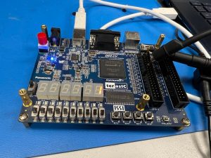
    • Debugged a lot of FPGA code using setup where FTDI code was connected to the FPGA, and laser receiver/transmitter connected via jumpers to each other.
  • Schedule
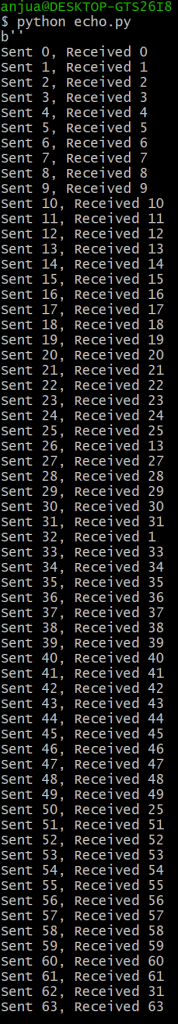
    • We are cutting into slack, but the core part of the project is done. We have moved onto integration and testing. In terms of work, this has transformed into adding/getting rid of debugging features for testing and design trade-offs. We have successfully transmitted a large file (19MB) over lasers, and reached MVP!
  • Next Week
    • Continue working on integration. See the best methods of transitions and talk about design decisions at full-scale level. Refine.
    • Work on design report/poster/presentation.

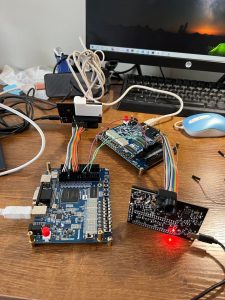
FPGA setup used for debugging

Anju Ito’s Status Report for 4/8/2023

  • Work this week
    • Integrated RAM use on the FPGA. Created a 1k FIFO using Quartus IP, and successfully integrated into the code. This fixed the error of not having enough logic components to compile the design on the FPGA, and instead using the embedded RAM on the chip.
    • Fixed a FSM logic bug that prevented the FPGA from transmitting 2 bytes in a row over the lasers.
    • Fixed timing issue for writes onto the FTDI chip. When testing with lasers, occasionally saw that the 6th bit in the byte was always a one. There was a logic error in the setup time that resulted in data not being held for an appropriate length before the write was asserted.
    • Finished writing code and loading all the files for demo. Created a board that can be configured to echo just using the FTDI chip and back, and another that transmits whatever it receives through the USB on the laser and writes back whatever it sees on the receiver back to the USB. Also attempted to test by turning the lasers completely off and on, board-to-board transmission (worked much more poorly then single board using mirrors), and turning ambient light filtering off (not work too well).
      • Attempting to fix the board-to-board by creating mounts for the PCB so that they are more stable.
    • Working through making the receiver more robust. Cleaned out logic, which may have made it slightly better. However, still occasionally see duplicates in numbers during laser transmission, which needs to be fixed/explained.
  • Schedule
    • Everything that we prepared for the demo we were able to show, although there are new issues such as the necessity of extremely precise alignments and receivers having errors that need to be addressed in the future. Everything is around 2 weeks behind schedule, as implementation is taking a longer time than planned.
  • Next Week
    • Attempt to make laser transmission code more robust. Currently seeing duplicates and wrong bits too regularly.
      • Potential solutions: Fix any bugs that exist, slow down transmission speed from 6.25MHz, change how the receiver is sampling, add real-life flaws onto simulation to attempt to get error, 3D printed mounts
    • Implement handshaking protocol.
    • Work with integration and start testing.
  • Testing/Verification
    • Unit Tests
      • Echo to test FPGA/FTDI/computer connection: Test that verifies the connection between FPGA to computer by computer writing/reading bytes, and the FPGA echoing that back through the FTDI.
        • Verified. Attempted to time, and realized that computer’s read function especially takes a long time to run, but the number of bytes read doesn’t affect speed.
      • Laser transmission test: Verifies that the whole pipeline from computer to FPGA to lasers work with single byte.
        • Verified. However, alignment changes results a lot, and multiple bytes become less stable.
      • Packet send test: NOT DONE. Send a full packet, and verify that it was received correctly on the other side. Should not load it onto the FPGA if the start sequence is not received properly.
    • FPGA Integration Tests
      • Stress Test: fill FTDI chip multiple times, see if it can process data appropriately
      • Speed Test: measure pin out speed with oscilloscope to verify laser transmission
      • Light Test: Try testing in different lighting environment to see that transmission works under reasonable room conditions
      • Distance Test: slowly move the boards away from each other. Adjust focus, and record the max distance bytes can be transmitted at.

Anju Ito’s Status Report for 4/1/2023

  • Work This Week
    • Wrote an echo program that reads bytes on the FTDI, and writes them back so it can be tested with computer software. Some bug exists with the reading, but communication has been established and it was seen that correct bytes can actually be read and written from the chip from both directions.
    • Continued to debug the FSM. Transitioning over to building smaller modules.
    • Attempted to transmit data at 6.25 Mbaud through laser. Sent it over FPGA, and received correctly on the board! Some bugs about reading, but verified that a single bit width can be detected and read.
    • Attempted to compile the Echo, and realized that 512 bits couldn’t be declared. Because that was the intended size for packets, realized that this needs to use built-in embedded memory on the FPGA, and created an IP that may be integrated and used instead. This can hold kbytes of memory, which is more than sufficient for our application.
  • Schedule
    • We were successful in verifying that both sides (lasers and FTDI chip) work to and from the FPGA. Next steps include debugging and building a more robust system, as well as integrating it into the full system. Things are behind schedule, partly as integration requires different projects and modules, which slows progress of FPGA development because they are not as modular as software.
  • Next Week
    • Figure out a code to put on the FPGA board during the demo
    • Make the memory work for the FPGA.
    • Fix bug for read write on FTDI.

Anju Ito’s Status Report for 3/25/2023

  • Work This Week
    • Designed, programmed, and compiled the FPGA FSM and datapath, though it needs much debugging work.
    • Got the simulation to run and wrote a testbench. The testbench did not work for a while due to syntax issues with ternary operations, but runs now and there are issues to debug.
    • Helped look at EEPROM programming to set the chip to 245 asynchronous FIFO mode using 9V 3A power delivery.
  • Schedule
    • The code is slightly behind schedule, and I hope to finish debugging the FSM through simulation by this week so that integration goes smoothly by the end of this week or next week.
    • By the interim demo, I hope to have a working FPGA code written. Although this cannot be demoed unless an FTDI chip and computer software is written. The basic sending data and receiving may be demonstrated as MVP.
  • Next Week
    • Finish debugging the full FPGA code through simulation.
    • Help out in other tasks as necessary, and possibly integrate with code/FTDI chip/lasers.

Anju Ito’s Status Report for 3/18/2023

  • Work This Week
    • Began to write FPGA code. Progress:
      • Wrote a laser transmitter module that will transmit 2 input data over 2 lasers if the data valid signal is set. This module will always transmit both data simultaneously. This is the desired behavior for the project, as our MVP will never use one laser and not the other.
      • Wrote a laser receiver module that always listens for a byte that follows UART protocol (start bit and stop bit). This module was configured so it can only receive both at the same time, and currently making different versions to test the receiver.
      • Debugged the laser transmitter and receiver by setting up the waveform viewer environment. This took some time, as the vcs compiler kept exiting on failure. It turns out that the source bashrc has to be called every time, and I have to make sure that I only have setup447 (or one of the class) and not the other, as those conflict with each other now.
      • Wrote an untested version of the FSM and protocol handler of the transmitter module.
    • Verified functionality of the transmitter and receiver modules by sending constant bytes from the transmitter to receiver using a single board, connected by jumper cables from the laser out line to the laser in line. Successfully sent bit, flashing the data received every time, and allowing for switches.
    • Imported pin configurations and assigned appropriate ones based on schematic. Modified code so that all GPIO pins except for transmitting and outputs are high impedance, and labeled/used each one for its set purpose.
    • Flashed the code successfully onto FPGA non-volatile memory. This involved emailing/creating a Terasic account to get their programmer, and converting file formats. This makes it much easier to just turn on the device without needing to reconfigure the board every time.
    • Integrated the FPGA with the PCB. Fixed issues with DNP resistor labelling that caused the FPGA to be turned partially on (3V3 was connected instead of the 5V to the FPGA. Fixed by removing and putting on the resistors). Verified that the lasers can be somewhat controlled by the FPGA, although there is no way to test it so far as the receiver did not work with preliminary testing using mirrors.
  • Schedule
    • Things are on schedule. Since boards have arrived and KJ has assembled them, my implementation from now will most on likely work in parallel with testing the board features and making sure that they will work. This will involve modifying the code and making a simplified version of it which would take some time, but also ensure that the code will work well with the board.
    • In addition, since there are potential issues with the receiver and we need to verify the functionality of the lasers, etc. I will use some time attempting to write test code and debugging that feature, which may slow down me working on FSM.
  • Next Week
    • Write out the full program for FPGA including the receiver FSM, and testing the transmitter FSM. Integrate it with the board and see how far I get.
    • Test out the laser transmitter/receiver on the PCB, because integrating with the FPGA may be the easiest way to test the board functionality, since it receives high speed transmission. Since it didn’t register the first time transmitting at 6.25 MHz using a mirror, potential things to do are slowing down this transmission speed greatly, using 2 boards for better laser power going to the other board, turning off ambient noise cancellation, and testing in a dark room.

Bits being transmitted and received by the receiver module (displayed on the HEX values, the first 2 for the IR receivers and the second 2 for the green receivers). The GPIO pins are connected with jumper cables.

Anju Ito’s Status Report for 3/11/2023

  • Work This Week
    • Significant amount of time was spent working on the design report this week, including FPGA implementations, diagrams, and overall project information.
    • Began coding modules for clock dividers that will be needed to time UART communication on the USB transceiver and laser side.
    • Came up with block diagram for the transceiver, consisting of 2 shift registers that will be enabled depending on number of bits that go into each.
  • Schedule
    • Design report took more amount of time than originally thought. Implementation will need to be worked on, which will hopefully be done the week after spring break.
  • Next Week
    • Have an overall implementation of all aspects of the FPGA, so that debugging can be conducted the week after using oscilloscopes for signal accuracy

Anju Ito’s Status Report for 2/25/2023

  • This week
    • Presented the design review for our team on Wednesday.
      • Worked on slides and practices beforehand.
    • Thought further about FPGA implementation, especially with regards to the interface between the FTDI chip.
      • For the FTDI chip, I had some concerns about using a single fast serial data that splits into 2 serial data complicating timing. As a backup plan and knowing options, I looked into potential other modes that the FTDI chip supports, and found the asynchronous FIFO mode. This was the only other option that seemed reasonable to use, as others supplied a 60MHz clock (faster than the FPGA onboard and will probably not go through the GPIO pins smoothly). I plan on attempting to implement the FPGA with the fast serial, but as a backup go into FIFO if there are timing issues that become difficult to smooth out. In addition, if speed of the fast serial becomes a bottleneck, this can also potentially allow for a much faster interface between the FTDI buffer data and the FPGA.
    • Thought through a little more of the block diagram and overall implementation, especially before the hardware arrives.
      • My plan is to have a rough implementation of the FTDI side, since some aspects are difficult to predict without the actual hardware in hand. I plan on working and refining more of the actual laser side since that can be read with the oscilloscopes through the GPIO headers to verify actions.
    • Helped focus the laser to verify that the laser beam angles can be fixed.
  • Overall schedule
    • I think that this week’s primary focus became the design review for the first few days. Although it’s not very far off schedule, I think that I could have worked on a more detailed implementation of the FPGA, which I plan on doing next week instead.
  • Goal for next week
    • Have an implementation of the laser side, and a rough idea of how the interface would be handled on the FTDI side on the FPGA.

Anju Ito’s Status Report for 2/18/2023

  • This Week
    • Tested speed of FPGA I/O pins from the Dev board to see how fast communication can go from custom PCB to the FPGA
      • Measured that 12.5MHz clock can cleanly be measured from the GPIO pins. From this, we decided that using an FPGA dev board was sufficient and a better option than a microcontroller. Faster speeds yielded questionable results, although there is a possibility that the oscilloscope probes couldn’t measure as fast. We can safely rely on using the 12.5MHz clock (i.e. 25 Mbps) communication for our project.
      • FPGA Spec
        • 50MHz clock
        • 3.3V active  high from GPIO pins 
      • Detailed measurements:
        • 4.15MHz from FPGA, measured with an oscilloscope at 500MS/s sampling:
          • 3.28V high, 0.096V low
          • 0.192V (3.472V) overshoot, 0.096V undershoot (3.184V)
          • Rise time: 4.6ns
          • Fall time: 4.0ns
        • With 6.25MHz, 200MS/s sampling:
          • 3.24V high, 0V low
          • 0.52V overshoot (3.76V, 3.24V base), 0.34V undershoot (2.9V)
          • Rise time: 9.0ns
          • Fall time: 8.75ns
        • With 12.5MHz, 500MS/s sampling
          • Very clean signal
          • Delta t = 12.5MHz
          • 0.200V overshoot, 0.12V undershoot
          • Rise Time: 4.4ns
          • Fall Time: 3.8ns
        • 25MHz, 500MS/s
          • Start to observe unclean signals
        • 50MHz

    • Worked with Roger and KJ to come up with communication protocol.
      • We weighed the different options between a SPI-based and a UART-based protocol, and concluded that we will use a UART-based protocol for LaserDrop, as this would yield better results after evaluating it while thinking about sampling speed from FPGA, circuit response, etc.
      • Decided on the packet properties of the laser communication (start sequence, packet ID, data, Hamming encoding, packet size)
      • Decided which aspects of our project (CPU, FPGA, circuits, COTS IC) would handle which part of the protocol
      • Came up with an error handling mechanism for lost packets
      • Came up with a handshaking mechanism for beginning/end of instantiating a communication
    • Designed the FPGA block diagram that would handle this communication.
      • Overall FSM and block diagram that will interface with the FTDI chip and PCB circuitry.
    • Worked on the design review presentation with the whole group.
  • Schedule
    • My work is on schedule. My goal last week was to test whether the FPGA dev board or the microcontroller would be able to support the communication, which I was able to do. Due to the success of how fast the signals came across from the FPGA board, we concluded that a microcontroller would be unnecessary and we can go forth with a custom PCB that would interface with the FPGA.
  • Goal for next week
    • Practice and present the design review during class.
    • Address the feedback/concerns that we receive during the design review from the advisors, faculty, and classmates
    • Refine and come up with a detailed FSM/block diagram of the whole system
  • Principles/Courses Used
    • 18-240, 18-341: In these classes, I learned how to use and design the FPGA boards (Altera DE0-CV), which I used to think about how the FPGA will interface with the FTDI chip and PCB circuits and handle the protocol that we designed. In addition, protocols such as the Hamming encoding and USB were explored in these classes that helped when we were coming up with the communication protocol. In addition, I wrote simple SystemVerilog code to test out the FPGA speeds, which I will heavily use later on in this project as well.
    • 18-349: Embedded Systems taught about various protocols such as SPI, UART, and I2C that we thought through while coming up with our custom protocol. In addition, 18-100 and Manchester encoding, etc. were another features that we thought about when thinking about the communication protcol.
    • MoonRanger (16-861/16-865: Space Robotics): Gave me hands-on experience with communication protocols (UART, etc.) that helped during protocol design. In addition, I learned and often used oscilloscopes and other tools, which made it easy for me to figure out the FPGA speeds.

Anju Ito’s Status Report for 2/11/23

  • Searched for FPGA/microcontroller options that were available for purchase
    • Found out that FPGA chip on a custom PCB would most likely be a difficult option. I was restricting the search to Altera chips (and non-BGA if possible), and found that most chips were out-of-stock or too old so that any recent version of Quartus does not support this.
      • The search was restricted to Altera due to my prior experience in 341/240.
    • Looked into a microcontroller that would have UART/SPI, that would enable communication from the FTDI (USB-UART chip) to the lasers. Filled out a purchase form for a MSP430 Launchpad. Estimated day of delivery was Monday if it were ordered yesterday.
      • KJ and I both have experience using MSP430 in the past, which is why we narrowed down the search to this.
      • We decided to get a dev board to test out its capability so we can make sure that it can support at least the 4Mbps communication to meet requirements.
  • Work is on schedule, although the unavailability of FPGA chips were unexpected and I would need to iron out the plan of handling the communication.
  • By next week, I hope to come up with a way to validate whether the microcontroller and FPGA dev board can support the communication requirements, and choose which design to proceed with based on this.