- Work This Week
- Began to write FPGA code. Progress:
- Wrote a laser transmitter module that will transmit 2 input data over 2 lasers if the data valid signal is set. This module will always transmit both data simultaneously. This is the desired behavior for the project, as our MVP will never use one laser and not the other.
- Wrote a laser receiver module that always listens for a byte that follows UART protocol (start bit and stop bit). This module was configured so it can only receive both at the same time, and currently making different versions to test the receiver.
- Debugged the laser transmitter and receiver by setting up the waveform viewer environment. This took some time, as the vcs compiler kept exiting on failure. It turns out that the source bashrc has to be called every time, and I have to make sure that I only have setup447 (or one of the class) and not the other, as those conflict with each other now.
- Wrote an untested version of the FSM and protocol handler of the transmitter module.
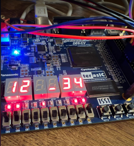
- Verified functionality of the transmitter and receiver modules by sending constant bytes from the transmitter to receiver using a single board, connected by jumper cables from the laser out line to the laser in line. Successfully sent bit, flashing the data received every time, and allowing for switches.
- Imported pin configurations and assigned appropriate ones based on schematic. Modified code so that all GPIO pins except for transmitting and outputs are high impedance, and labeled/used each one for its set purpose.
- Flashed the code successfully onto FPGA non-volatile memory. This involved emailing/creating a Terasic account to get their programmer, and converting file formats. This makes it much easier to just turn on the device without needing to reconfigure the board every time.
- Integrated the FPGA with the PCB. Fixed issues with DNP resistor labelling that caused the FPGA to be turned partially on (3V3 was connected instead of the 5V to the FPGA. Fixed by removing and putting on the resistors). Verified that the lasers can be somewhat controlled by the FPGA, although there is no way to test it so far as the receiver did not work with preliminary testing using mirrors.
- Began to write FPGA code. Progress:
- Schedule
- Things are on schedule. Since boards have arrived and KJ has assembled them, my implementation from now will most on likely work in parallel with testing the board features and making sure that they will work. This will involve modifying the code and making a simplified version of it which would take some time, but also ensure that the code will work well with the board.
- In addition, since there are potential issues with the receiver and we need to verify the functionality of the lasers, etc. I will use some time attempting to write test code and debugging that feature, which may slow down me working on FSM.
- Next Week
- Write out the full program for FPGA including the receiver FSM, and testing the transmitter FSM. Integrate it with the board and see how far I get.
- Test out the laser transmitter/receiver on the PCB, because integrating with the FPGA may be the easiest way to test the board functionality, since it receives high speed transmission. Since it didn’t register the first time transmitting at 6.25 MHz using a mirror, potential things to do are slowing down this transmission speed greatly, using 2 boards for better laser power going to the other board, turning off ambient noise cancellation, and testing in a dark room.

Bits being transmitted and received by the receiver module (displayed on the HEX values, the first 2 for the IR receivers and the second 2 for the green receivers). The GPIO pins are connected with jumper cables.
