
Accomplishments
I’ve spent the past week writing all of the documentation that we will need to implement the Hardware side of the project without having to answer any new questions. I’ve also written the Transport Layer Protocol, which is the contract that Mark and I will use to have our components communicate when we implement our respective modules.
The transport layer specification is hosted here:
https://docs.google.com/document/d/1I2FRMwITUbSbkqIw_w6eQ5OyxKJneer853xGVAFtx5I/edit
I’ve designed a bunch of necessary diagrams this week:
- Top-Level Block Diagram
- Model Manager FSM
- Job Manager FSM
- Module interfaces for:
- Data Pipeline Router <-> Model Manager
- Model Manager <-> FPU Bank
- Data Pipeline Router & Model Manager <-> Memory Management Unit
Here are some of the FSMs to be implemented in Hardware:
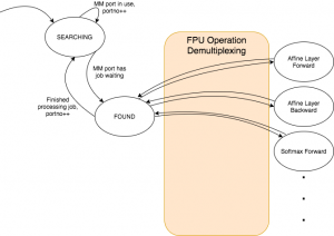
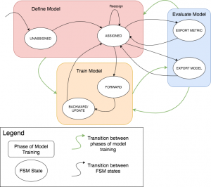
These are the FSMs for the Job Manager and the Model Manager seen in our Top-Level Block Diagram.
In addition, we now know what module-level interfaces will look like:
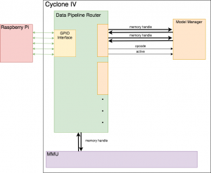
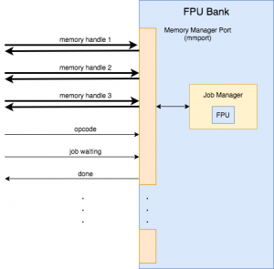
One important thing to note is that we’re labeling many arrows as “memory interfaces”. This goes back to the mentality of passing pointers instead of data between modules, since we want to copy data as few times as possible (again, training a model is a memory-hard problem). A memory handle will be a Verilog struct with at least the following connections:
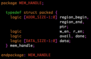
These logic values are direction-agnostic, meaning we don’t care if different modules are writing to different wires in the same struct, as long as there are no write-write conflicts. Passing a mem_handle struct from one hardware module to another will be equivalent to passing a pointer in C — it basically exposes a region of memory to a module, so that the module itself can be completely agnostic to where in memory it is working. The idea with this is that the Memory Managers will store mem_handles in registers, and selectively expose these to Job Managers in the FPU Bank when it needs to perform some computation.
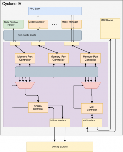
Another important design decision that I’ve made is to set up the MMU to use both the on-chip M9K blocks and the Off-chip SDRAM. When we were making our Project Proposal, we assumed that memory would not be an issue because we could synthesize more if necessary. That was a naive workaround, and this method is better. We still intend to synthesize a cache for each Memory Port controller to quickly serve reads and cache data read from SDRAM, but the bulk of weight memory and intermediate memory will need to be stored off-chip. As of now, we plan on using an SDRAM controller that services requests to read from and write to memory in a round-robyn fashion.
Schedule
When we made the Gantt chart for our Project Proposal, we divided the hardware component into three parts (FPU Bank, Data Pipeline Router, and Model Manager) and split those into separate weeks under the assumption that I could sit down, write one module, and never have to look back at it. We neglected the need for a comprehensive design document, and in doing so neglected to plan for an extra MMU. Having done all this design is extremely helpful, but I also realized I need to seriously rewrite my portion of the Gantt chart. That will be happening in the next couple of days and will be done on Monday.
Accomplishments For Next Week
By Tuesday, I will be completely done with all of the design documents for the hardware worker (excluding the GPIO protocol and Data Pipeline Router handshake, since those are Jared’s responsibility). With the documentation done, I’m going to start finding any code I can clone for use in our project. Basically, I will implement basic FPU operations, have an SDRAM controller (I can copy the one I wrote in 18-341), and I will hopefully have an M9K controller. With all of these modules done, we’ll have all of the “Unknown Unknowns” out of the way for the hardware side, and all of the remaining tasks will be things that we know how to do and are well-documented.