18-348 Lab #10
Spring 2016
This lab is based on Lecture 19 - Analog Outputs and Lecture 20 - Analog
Inputs.
Links to all files referenced in the lab and prelab can be found in the
Files section at the end of this document.
NOTE: It is important to rename your source code files to include your andrew ID for prelab and your group number for the lab. This applies to any main.c, main.asm, and other files you are handing in.
Navigation
Prelab - Analog I/O
Lab - A/D conversion and PWM
Support Materials
Goal:
- To learn about and implement analog I/O.
Discussion:
Refer to the lectures on D/A and A/D conversions.
Resolution is defined as "the smallest distinguishable change in
input ... that causes the digital output to change by 1" (Valvano,
p. 573).
|
Note that the equations on p. 368 of the MCU datasheet are missing a newline. The page should say:
- Left aligned output (CAEx = 0)
- PWMx period = channel clock period * PWMPERx
- Center aligned output (CAEx = 1)
- PWMx period = channel clock period * (2 * PWMPERx)
That is, the first equation is for left aligned output, and the second equation is for center aligned output. The correct equations can also be found in sections 12.4.2.5 and 12.4.2.6 (p. 379/381). In general assume we are using left-aligned output unless otherwise stated.
|
Procedure:
Answer the questions below.
Questions:
Part 1:
Q1: State the period and duty cycle for each waveform shown in
Figure 1. Assume the figure is to scale in the horizontal
dimension. Assume that all signals are periodic.
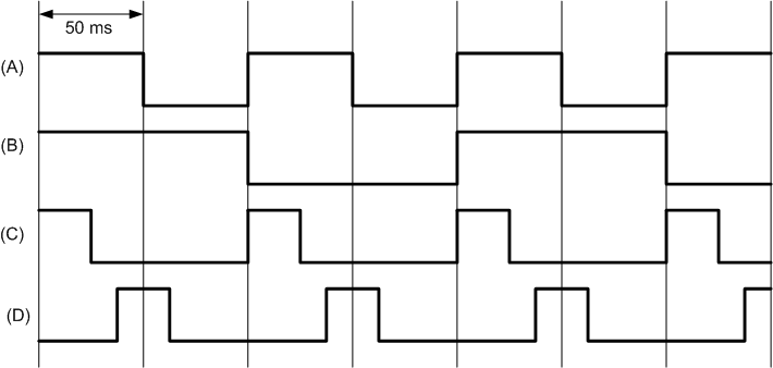
Figure 1: PWM Waveforms
Part 2: Resolution
Read section 12.3.2 and 12.4 of the MC9S12 datasheet and answer the
questions below. PWM output is controlled by an 8-bit duty cycle register
and an 8-bit period register.
Q2: What is the period of a waveform generated, given a PWM clock
set to 0.5 MHz with a left-aligned, positive polarity waveform, and
PWMPERx=0xFF? What is the resolution of the analog output? Give
your answers in microseconds. (Hint: The resolution is the smallest
change in the width of the positive pulse achievable by changing the PWMDTYx
register).
Q3: Given the example in question 2, but with a PWM clock of 1 MHz,
what is the period? What is the resolution? Does having a smaller
resolution allow you to achieve a more accurate duty cycle? (Note: it is
important for this question to keep in mind that duty cycle is by definition a
ratio.)
Q4: What is the resolution of a basic A/D converter, in terms of Vdd
(the reference voltage) for a 10-bit conversion? for an 8-bit
conversion? How does this compare to the reference values given in
section A.2 of the MC9S12 data
sheet? Hint: look at tables A-12 and A-13.
Hand-in Checklist: (60 points)
All non-code submissions shall be in a single PDF document.
All code submissions shall have Andrew ID in the filename
- (60 points) Answers the the questions above; 15 points each. SHOW YOUR
WORK when answering questions.
Refer to the LAB FAQ for more information on lab
handin procedures and file type requirements. You MUST follow these
procedures or we will not accept your submissions.
Goal:
- In this lab, you will use A/D conversion to read analog inputs and the onboard PWM module to produce analog outputs.
Discussion:
There are several ways to control the brightness of an LED. One is to
adjust the series resistance, since the brightness is proportional to the
current. However, digitally controlled potentiometers are expensive and
not very robust. A much simpler solution is to pulse-width modulate the
LED. By turning the LED on and off repeatedly at high frequencies, the
average brightness of the LED is reduced. The human eye is unable to see
the high-frequency flashing so long as it isn't too slow, so the LED appears to
be steady, but dim.
In this lab, you will convert an analog input to a PWM output on Port P0 to
control the brightness of the LED. You will use digital outputs on the
LS138 chip to route the PWM signal to various LEDs, so that you can implement a
variable-brightness LED chaser. Note that the Port T1 output is tied to
the active-low input G2B*. This allows the MCU to be able to enable /
disable the LED output.
In addition, you will use a second analog input to control the rate at which
the LEDs chase. You will use the analog input to adjust the compare value
for the onboard timers. Using timers in compare mode is slightly
different than the way we have used timers in previous labs. In output
compare mode, an interrupt is generated when the TCNT register reaches a
certain compare value (TCx). The compare event can generate an interrupt,
and in the interrupt you can adjust the digital outputs to the LS138 decoder
accordingly.
For additional information about configuration register for the ATD module,
PWM module, and Timer module, consult sections 8, 12, and 15 of the
MC9S12 data
sheet . You should be used to figuring out the configuration of the
MCU using control registers. In the lab, you will be expected to figure
out the correct configuration on your own. Although the data is all there
in the datasheet, do not wait until the last minute! Be sure to leave
yourself plenty of time for testing and debugging.
Procedure:
Part 1: A/D and D/A Implementation
The program you implement shall meet the following requirements:
- The program shall follow the configuration guidelines found in the comments
in the skeleton file.
- The LCD panel shall display the current result of the AD0 and AD1
analog-to-digital conversions, updated at least every 200ms.
- The 8-bit digital conversion result of the analog panel-mount potentiometer
shall be used to set the 8-bit duty cycle value of the PWM output.
- At minimum duty cycle (corresponding to analog input ~=0V), the LEDs shall
be turned off. I.e. the minimum duty cycle shall be 0%.
- At the maximum duty cycle (corresponding to analog input ~=5V), the LEDS
shall be turned on for the entire duration of the chase period. I.e. the
maximum duty cycle shall be 100%
- The LED chase rate shall be defined as the amount of time from when an LED
is first lit to the time when that LED is lit again after the LEDs have gone
through one cycle.
- The rate at which the LEDs chase shall be a function of the analog input
from the potentiometer on the project board.
- The minimum rate (corresponding to the analog input ~=0V) shall be 100ms
+/- 5 ms.
- The maximum rate (corresponding to the analog input ~=5V) shall be 1000ms
+/- 5ms.
- The rate between the minimum and maximum values shall be a linear function
of the analog input.
- When the PB1 button is pressed, the LED chaser shall pause, but the
brightness control shall continue to function.
Follow these steps to implement the program described above.
- Wire your board according to the Lab 10
Schematic.
- Download the lab_10_skeleton.c file and
rename it to lab_10_gxx.c.
- Create a new C project replace the main program with lab_10_gxx.c.
Add the
lcd_lib-1_2 and
modclock files to your project.
- Implement the program. Be sure to follow the requirements above,
especially following the comment guidelines given in the skeleton file.
- Test the program to make sure it meets the requirements described above.
- Q1. Hold down the pause button (PB1) and adjust the brightness of
the LED using the panel-mount potentiometer. For each range in Table 1
below, record the range of values for each of the subjective brightness
views. It may help to turn out the lights or stand a piece of paper up
next to the LEDs when doing this part. An example value has been included
in the table. Do NOT use this value in your results.
Subjective Brightness
|
Range of A/D conversion results
|
Off
|
0x00-0xB3
|
Very Dim
|
|
Dim
|
|
Bright
|
|
Very Bright
|
|
Extremely Bright
|
|
Table 1: Subjective brightness of LEDs
Part 2: Analog input and output measurement
- Connect the oscilloscope to test point 2 and configure the oscilloscope to
trigger on a rising edge of that signal. You will be observing the PWM
output from the MCU.
- Measure the voltage at Test Point 1. You may use the a
multimeter or another channel of the oscilloscope. Note that of the max
and min duty cycles, there will be no edge to trigger on, so you will have to
measure the analog voltages in these cases with a multimeter or find a way to
force a trigger on the oscilloscope.
Q2. Adjust the panel mount potentiometer (analog input) until the value displayed on the LCD matches the value in the first row of Table 2
below. For each row of the table, record the analog voltage and the duty
cycle of PWM output. A sample entry has been included. Do NOT use this
sample entry in your data.
- Q3. Graph analog input voltage vs. the digital conversion value.
- Q4. Graph the digital conversion value vs. PWM duty cycle.
Analog Input Voltage (V)
|
Digital representation of AD0 (#)
|
PWM Duty cycle (%)
|
.001 V
|
0x00
|
0
|
|
0x01
|
|
|
0x02
|
|
|
0x03
|
|
|
0x04
|
|
|
0x05
|
|
|
0x10
|
|
|
0x20
|
|
|
0x30
|
|
|
0x40
|
|
|
0x50
|
|
|
0x60
|
|
|
0x70
|
|
|
0x80
|
|
|
0x81
|
|
|
0x82
|
|
|
0x83
|
|
|
0x90
|
|
|
0xA0
|
|
|
0xB0
|
|
|
0xC0
|
|
|
0xD0
|
|
|
0xE0
|
|
|
0xF0
|
|
|
0xFC
|
|
|
0xFD
|
|
|
0xFE
|
|
|
0xFF
|
|
Table 2: Analog inputs, intermediate digital value, and analog output.
Part 3: Chase loop timing measurement
- Connect an oscilloscope lead to test point 3. Configure the
oscilloscope to trigger on a falling edge on this input. You will see a
series of negative pulses in the signal. Each of these pulses represents
the first LED in the sequence being turned on.
- Q5. Measure the period of the LED chase sequence for each value of
AD1 listed in Table 3 and record the results in the table. A sample entry
has been included. Do NOT use this sample entry in your data.
- Q6. Graph the the digital AD1 value vs. the LED chase period.
Digital representation of AD1 (#)
|
LED Chase Period (ms)
|
0x00
|
100ms
|
0x10
|
|
0x20
|
|
0x30
|
|
0x40
|
|
0x50
|
|
0x60
|
|
0x70
|
|
0x80
|
|
0x90
|
|
0xA0
|
|
0xB0
|
|
0xC0
|
|
0xD0
|
|
0xE0
|
|
0xF0
|
|
0xFF
|
|
Table 3: Intermediate digital value and LED chase period.
Part 4: 16-bit PWM
In this part, you will reconfigure the PWM for 16-bit resolution.
NOTE: Since the 16-bit PWM defaults to outputting on PTP1 you must either move the wire from PTP0 to PTP1 or use MODRR to reroute PWM1 to PT1 (which is already connected in the schematic) to connect the output in this part. Either method is fine.
- Make a copy of your lab_10_gxx.c. Name the copy lab_10_16bpwm_gxx.c
and use it for this part of the lab.
- Modify the original program to meet the following constraints.
- Modify the LED chaser to run at a fixed rate of 1 second per chase
cycle. Modify the digital outputs on Port P so that the PTP1 is
configured for PWM1 and PTP0 is always high. (The last part is necessary
to keep the LEDs enabled).
- The pause button must have the same effect as previously.
- Configure the PWM module to concatenate PWM channels 0 and 1 into a single,
16-bit PWM. Note that this requires you to use PWM1 as an output.
- Configure the PWM to use 0 polarity. This is necessary
because the PWM1 output is connected to an active low enable.
- Set the PWM period to 0xFFFF.
- Change the PWM clock to run at the bus clock rate (8 MHz).
- Set the most significant byte of the PWM duty cycle to the digital
conversion result from the potentiometer input on the project board
(AD1). Set the least significant byte of the PWM duty cycle to the
digital conversion result from the panel-mount potentiometer (AD0).
- Connect the oscilloscope to Test Point 4 (or point 2 if you're using PTP1) and configure the oscilloscope to
trigger on the FALLING edge. We use the falling edge because we're using
the opposite polarity.
- Q7. Adjust the two analog inputs and observe the effect on the
brightness of the LED. Which analog input gives fine-grained control of
the PWM duty cycle? Which analog input gives course-grained control of
the PWM duty cycle? Explain this in terms of which input controls which
byte of the PWM duty cycle register.
- Q8. Use the oscilloscope to measure the duty cycle. Record the
change in duty cycle for one step change (e.g. change from 0xF0 or 0xF1) in the
coarse-grain analog. For the fine-grained input, recored the change in %
duty cycle when you go from 0x0 to 0xFF and divide this value by 255 to get the
appropriate single step value. Record the change-in-%-duty cycle for 1
step in each analog input. Compare these measured values to the
theoretical values and explain a possible source for any difference.
Bonus -- Part 5: Etch-a-sketch (Optional)
For this bonus, implement an
etch-a-sketch with the
following requirements:
1. The visual output of the etch-a-sketch shall appear on an oscilloscope
screen.
2. The oscilloscope shall be set to X-Y Mode operation (Refer to the
oscilloscope reference manual for more details)
3. The module / project board shall output the X and Y positions of the cursor
as two PWM outputs
3.1. The PWM outputs shall act as inputs to two corresponding RC circuit
filters.
3.2. The outputs of the RC filters shall be the inputs to the oscilloscope.
4. The user shall control the cursor position on the oscilloscope screen using
two potentiometers connected to analog inputs of the module (one for the X
position and one for Y position).
The oscilloscopes in the lab are Agilent Technologies DSO6012A. The manual is available
here: Agilent 5000/6000/7000 Series Oscilloscopes User Guide.
Demo Checklist: (80 + 8 points)
- (20 points) Demonstrate to the TA that your program lab_10_gXX.c meets all
the requirements given in the lab and code skeleton.
- (20 points) Use the oscilloscope to demonstrate to the TA that the
brightness control covers the whole range of PWM duty cycles.
- (20 points) Use the oscilloscope to demonstrate the minimum and maximum LED
chase periods.
- (20 points) Use the oscilloscope to demonstrate both course and
fine-grained control over the PWM period.
- Bonus: (8 points) (Optional) Demonstrate your oscilloscope etch-a-sketch to
the TA.
Hand-in Checklist: (155 + 15 points)
All non-code submissions shall be in a single PDF document. Each graph must
have a title, your names, and correct, appropriate labels (describe the axis
and give units, if any) to receive full credit.
All code submissions shall have group name in filename
- (5 points) List any problems you encountered in the lab and pre-lab, and
suggestions for future improvement of this lab. If none, then state so to get
these points.
- (50 points) Submit your final version of lab_10_gXX.c. You must
follow the Coding style sheet to
receive full credit.
- (5 points) Q1 (Table 1)
- (20 points) Q2 (Table 2)
- (5 points) Q3 (graph)
- (5 points) Q4 (graph)
- (15 points) Q5 (Table 3)
- (5 points) Q6 (graph)
- (30) Submit lab_10_16bpwm_gxx.c. You must follow the
Coding style sheet to receive full
credit.
- (5 points) Q7
- (5 points) Q8
- (5 point) How many hours did each team member spend on the class (including class time) between 10 April and 17 April. Do not include time spent working on bonus problems.
This replaces the weekly data collection we normally get from quizzes.
- (Bonus: 15 points) Implement the etch-a-sketch in part 5. Submit your
code as lab_10_etchasketch_gxx.c. You must follow the
Coding style sheet to receive full
credit.
Refer to the LAB FAQ for more information on lab
handin procedures and file type requirements. You MUST follow these
procedures or we will not accept your submissions. SHOW YOUR WORK when
answering questions.
FILES for this lab:
Relevant reading:
Also, see the course materials
repository page.
Change notes for 2016:
- 3/20/16 - Added navigation and notes about filenames -- Milda