18-729 High-Frequency Analog IC
Design and Device Modeling
Tutorial on Cadence Design Tools
Ruifeng
Sun
(ruifengs@ece.cmu.edu)
![]()
In 18-729, we will use
Cadence tools to do transistor-level circuit design and simulation. Cadence provides a powerful integrated
working environment for analog/digital/mixed-signal integrated circuit design,
simulation, layout and verification.
For more information, please refer to its official website: http://www.cadence.com. For the purpose of this course, we will only
focus on those tools relevant to analog and RF integrated circuit design.
This tutorial will cover
most of the features that is sufficient for you to finish 18-729 homework
assignments and design projects. It is
divided into two parts:
·
Part I: Setting up your
environment in ECE machine. Please
carefully follow this section to start Cadence correctly, since various
versions of Cadence currently co-exist in ECE machines.
·
Part II: We will go
through an example to simulate the noise figure of a passive bridge-T
attenuator, which is actually a question in homework #1. We will also talk about how to get more help
from Cadence
Even though you are already
familiar with Cadence to do RF IC design and simulation, you will still need to
read Part I.
Part I. Environment Setup
1.
First of all, you need
to have an ECE account. If this is not
true, please contact ECE computing service: gripe@ece.cmu.edu.
2.
If you are using a
Windows workstation, you need to make sure you have an X-window server ready
(most likely, the software is X-win32); and after logging in to an ECE server,
you should setup a display environment variable with this command:
>setenv
DISPLAY the name of the machine you are
using:0.0
3.
Create a directory
where you want to save your work, for example, ece729:
>mkdir ece729
4.
Enter the directory you
just created:
>cd ece729
5.
Run this command:
>/afs/ece/class/ece729/cadence/cds729
6.
Wait for a while, and
the CIW window of Cadence should pop up.
If not, please check if you have followed the above procedures.
7.
Next time to start
Cadence, enter the directory where you saved your old designs (i.e., ece729 in above example), and type and
run this command:
>./cds729
You can find all devices (transistors, resistors,
capacitors and inductors etc.) needed in a standard device library called
“analogLib”, which is provided by Cadence.
For transistors, you will need device models. The models we are going to use in this class come from
TSMC-0.18μm CMOS process. The
model file is “tsmc018.scs”, which
should already be copied to your working directory (i.e., ece729 in above example) if you follow above procedures
correctly. It contains several sections
to account for different process corners.
We will use the typical process parameters, so you need to specify
section “tt” when you set up model
libraries for the simulation later on in Cadence.
Part II. An Example
In this section, we will find the noise figure of a
bridge-T passive attenuator, and briefly introduce how to get help from Cadence
documentations.
1.
As Cadence is running,
in the CIW (Command Interpreter Window), click “File > Open…” in the menu
bar.
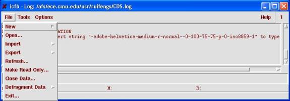
Figure 1. Cadence CIW window
2.
The “Open File” window
will pop up. Select “Library Name” as
“test”, and choose “bridge-T” as “Cell Name” from the list at the right
side. Make sure “View Name” is
“schematic”. Click “OK”.
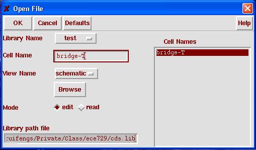
Figure 2. Open File Window from CIW
3.
The “Virtuoso Schematic
Editing” window will appear, and you will see a bridge-T passive attenuator,
which simply consists of three resistors.
There are also two additional instances “PORT0” and “PORT1”.
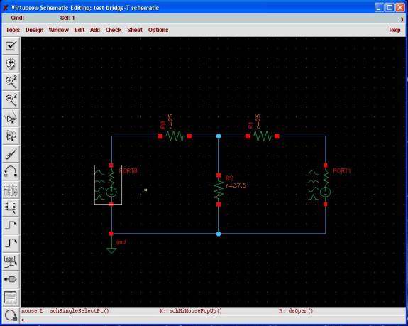
Figure 3. Virtuoso Schematic Editing Window
4.
Here are some basic schematic
editing shortcuts you should know: To select an instance, simply point and
click on it. To insert a new instance,
press “i” and you will see a new window named “Add Instance” (Figure 4). Fill in proper “Library”, “Cell” and “View”
names, and click on the schematic window, you finish to insert a new instance,
and you can press “Esc” to close “Add Instance” window. To delete the instance, first select it and
then press “d”. To change the
properties of the instance, first select it and then press “q”; an “Edit Object
Properties” window (Figure 5) will open, and you can modify the properties of
the instance. To copy an instance,
first select it, press “c”, and then click in a blank area in the window. To rotate an instance, first press “r” and
then click it. To flip an instance,
first select it, press “m”, and then press “R”. To wire the devices together, press “w” and click the two points
you want to connect. To undo what you
have done, press “u”. All of these
commands can be found in the “Edit” menu.
These shortcuts are summarized in Table 1.
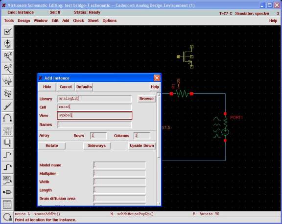
Figure 4. Add Instance Window
Table 1. Commonly-used Shortcuts for
Schematic Editing
|
Shortcut (keyboard) |
Action |
|
i |
insert new instance |
|
d |
delete instance |
|
q |
modify the
properties of an instance |
|
c |
copy an instance |
|
r |
rotate an instance |
|
m + R |
flip an instance |
|
w |
connect two nodes |
|
u |
undo |
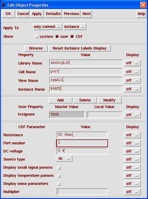
Figure 5. Edit Object Properties Window from Virtuoso
5.
Let’s go back to the
“Virtuoso Schematic Editing” window. In
the menu bar, click “Tools > Analog Environment”, and a new window called
“Cadence Analog Design Environment” will appear.
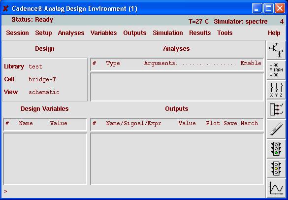
Figure 6. Cadence Analog Design Environment Window
6.
In the menu bar, click
“Setup > Model Libraries …”. Another
window called “Model Library Setup” pops up.
Click “browse” button, and you will see a new window similar to a file
browser. Choose “tsmc018.scs”, and
click “OK”. The browser closes and we
return to the “Model Library Setup” window.
Don’t forget to fill “tt” in the “Section (opt.)” field! Click “Add”, and then click “OK”. The “Model Library Setup” window closes and
we return to “Cadence Analog Design Environment” window. By the way, we actually don’t need any
device model for this example, since we only use ideal resistors and
ports. However, you certainly will need
this step in most of your home assignments and design projects.
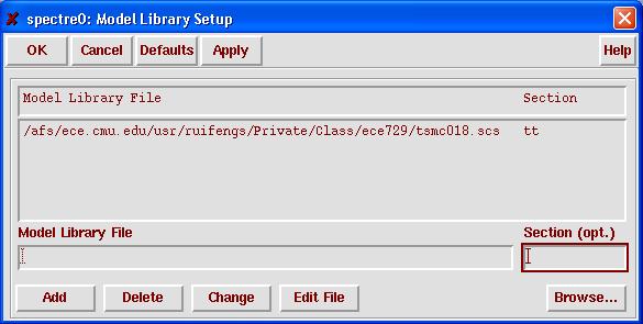
Figure 7. Model Library Setup Window
7.
Now we are in “Cadence
Analog Design Environment” window.
Click “Analyses > Choose …” in the menu bar, and “Choosing Analyses” window
will appear. Check “sp” in the
“Analysis” list. You will see the
content of the lower half window changes as you choose different analyses. Now, we are going to setup the parameters
for an “S-Parameter Analysis”. Click
“Select” button in the “Ports” field, and then click on instances “PORT0” and
“PORT1” in the “Virtuoso Schematic Editing” window. Press “Esc” before you return to “Choosing Analyses” window. You now should see the “Ports” has been
filled with “/Port0 /Port1” as shown in Figure 8. Select “Sweep Variable” as “Frequency”. Select “Sweep Range” as “Start-Stop”, and fill “Start” and “Stop”
with “1k” and “1G”, respectively. This
means we will sweep the frequency range from 1-kHz to 1-GHz. Choose “Sweep Type” as “Logarithmic” from
the drop-list, check “Points Per Decade”, and fill the blank field with
“100”. Check “yes” for “Do Noise”. Select “Output port” by first clicking
“Select” button and then in the schematic window clicking “PORT1”. Do the same to select “Input port” as “PORT0”. The finished “Choosing Analysis” window will
look as that shown in Figure 8.
Finally, click “OK”.
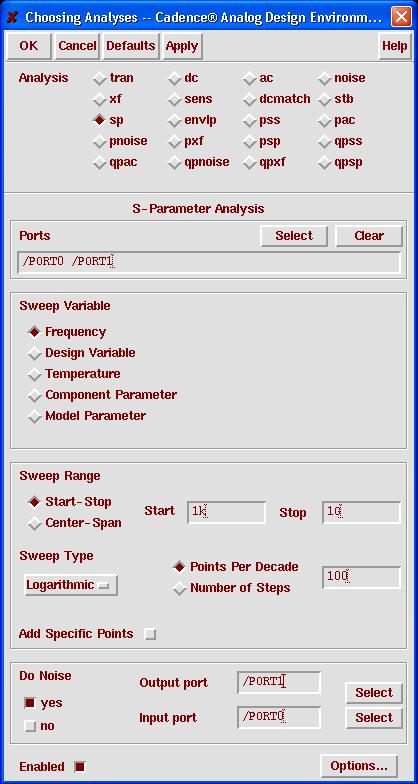
Figure 8. Choosing Analysis Window
8.
Now, we return to
“Cadence Analog Design Environment” window.
At the right side of the window, you will find a column of buttons. Click the one like a traffic signal with
green light. The function of the button
will show up as you place your mouse on it.
So, as you can see, we are going to “Netlist and Run” the
simulation. Wait for a second, Cadence
will first generate the netlist of the circuit and then run the
simulation. As the simulation is
running, a new window (Figure 9) pops up and let you know the progress of the
simulation. It won’t take a long time
to finish, and you can look for such a sentence in the CIW window:
“simulation completed successfully.”
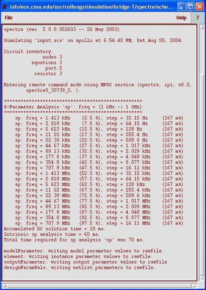
Figure 9. Output Log
Window
9.
Going to “Cadence
Analog Design Environment” window, in the menu bar, choose “Results > Direct
Plot > Main From …”. A “Direct Plot
Form” window will pop up. Check “NF”
from the list of the “Function”. Check
“dB10” as the “Modifier”. Click “Plot”
button. A new “Waveform” window will
appear, and the noise figure of the bridge-T attenuator against the frequency
will be plot in this window.
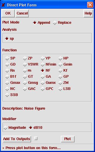
Figure
10. Direct Plot Form Window
Now, we finish our simple example. In fact, all of above procedures can be
found in Cadence help documentation.
There are two ways to open the help documentation: (1) type and run
“cdsdoc &” in your command line; (2) in the CIW window, click “help >
Cadence documentation”. In either way,
after waiting for a while, you will see a new window. Choose “Docs by Family” in the second pop-up menu. Double click on “Analog & Mixed-Signal
Design”. Find and double click on
“Spectre RF User Guide”. Double click
on “Table of Contents” and a web-browser will open. Look for the chapter of “Simulating Low noise amplifier”, and
look at the section of “Linear Two-Port Noise Analysis with S-Parameters”. You will find what we just discussed to do a
noise-figure analysis. “Spectre RF User
Guide” contains all aspects of RF IC simulation, and the best of all, it has
step-by-step examples to help you to simulate LNA, Mixed, VCO etc. You are suggested to spend some time on it
to get familiar with those topics.
Good luck!