This week I worked on making the final presentation slides with Amelia. I also worked on integrating the PCB as part of the whole system with the Verilog team. I also fixed some of the soldering work on a LED that wasn’t working too well – the “i” on the lampboard – by desoldering it and moving to another pin on the shift register.. Finally, I continued working on the final report.
Author: tsethi2
Tanisha’s Status Report for 4/19
This week I finished soldering our PCB and conducted PCB testing. I also started working on integration with the Verilog team.
I conducted extensive PCB testing throughout the week. I checked continuity for every connection on the board, checked each pin was supplying the appropriate power level, and power level at every connection and ensured it matches the schematic.
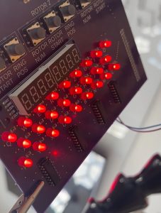
I also powered the PCB to ensure things were functioning and found all but one LED was working. I fixed this by trying to resolder the PCB, however in doing so I accidentally ruined a pad of the LED. However, I didn’t realise this at first so I worked on figuring out if the issue was with a dead LED, dead shift register, or a power issue.
By checking continuity and power outrages throughout the traces along the path of the power -> LED -> resistor -> ground, I was able to isolate the issue to be a lack of connection around the LED, hence realizing the pads were ruined. I solved this by incrementally soldering bare wire between the connections I wanted (power -> LED and LED -> resistor) till all connections were verified by both tests and finally the LED started working! The benefit of all of this means I am confident in the rest of my connections due to all of the debugging I did.
This is an example of skills I have learned over this past semester – trial and error by practicing my soldering and circuitry skills. I also learned more skills by asking other capstone groups for advice if they had encountered similar situations, I would say that was one of the most beneficial learning experiences I had. I also had practice outside of Capstone with TAing 18-349 where I had plenty of practice on laying out / fabricating and soldering PCBs.
The only task I have left for the PCB is fixing the rotary encoder as I laid the order of the pins out backwards on the schematic accidentally. I looked into a perf board solution to remedy this, but ultimately decided on adding another right angled header to try and change the direction of the encoder. I will also work on our final presentation and documentation for our final few submissions.
Team’s Status Report for 4/12
Two weeks ago we had our Interim Demo and received good feedback from this. We presented a working encryption scheme with inputs on the PS/2 keyboard and output displayed to the FPGA’s 7 segment display and using the FPGA switches as rotor dupes, a printout of our PCB with components laid out (since PCB was still being manufactured), and a presentation with our updated use case, design, and schedule. We felt that this Demo went well and based on feedback plan to update our final Demo to have 2 separate models – one with only the FPGA and one with both the FPGA and PCB to show off all the work we have done till now.
This past two weeks Amelia and Nancy worked hard on the rotary encoder RTL, wrote the entire SPI protocol for the MAX7219 7 segment display and integrated the encryption modules to work with all of the GPIO RTL they have written over the past few weeks and got everything working successfully!!
This week the PCB arrived (yay! see attached picture!) so Tanisha fabricated it and soldered all the SMD and PTH components on excluding the rotary encoder. Once that header arrives on Monday, she can solder it and the PCB fabrication will be complete. This week she will work on testing the PCB, completing her final report tasks and starting preparation for the final presentation.
For validation we will test our integrated system against results from each of our modular subsystems continuing on from our individual verification tests.
Meanwhile, the Verilog team will work on integrating the rotary encoder with the rest of the RTL and writing the RTL for the lampboard shift registers.
After the RTL is complete, the whole team will work on integrating the PCB with the RTL, carrying out user testing and planning the final demo set up. This all fits in to our planned schedule!
Tanisha’s Status Report for 4/12
This past two weeks I worked on preparing for our interim demo, working on PCB manufacturing tasks and other odd items.
I ordered our stencil from OshStencil. I ran into a few issues with trying to resize our stencil as it was charging us for a lot of negative space even though I didn’t need those extra sq inches. However, I was able to order it and it arrived successfully.
Since our stencil hadn’t arrived for the earlier part of this week, I worked on writing encodings to our Micro SD cards and making sure everything was formatted correctly, and running storage tests. I pivoted from using H2testw to f3 testing so I would be able to check storage sizes as well as corrupt disks.
I also started working on our Final report – specifically the PCB section as that is solely my responsibility as well as updating the Ethics session of our paper based on our Ethics lecture notes and previous status reports.
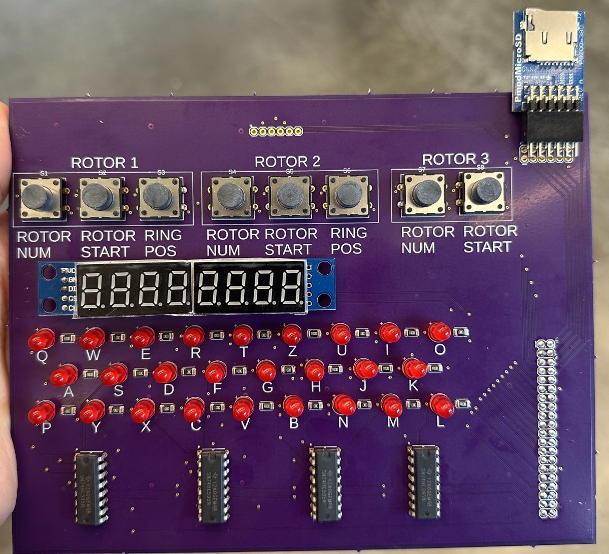
On Friday the PCB arrived (yay!). I immediately fabricated the resistors in the Fab Lab in Techspark and on Saturday I hand soldered the LEDs, 7 segment display, shift registers, FPGA header and the SD card reader and its right angled header. This comprises the majority of our PTH components.
I ran into slight issues as I had planned to desolder the right angled headers that came with the rotary encoder for a clean look and to balance the center of gravity for our users. However, that was proving tricky and I didn’t want to mess with the rest of the board as we got the last 2 rotary encoders in stock and hence have no spares. Due to this, I tried to source right angled female headers on campus but ended up just ordering some. Once these arrive, I can solder the rotary encoder and with that the PCB fabrication would be complete. I have attached a picture of the current state of the PCB to this status report.
This week I plan to run more continuity tests (I did small modular testing as I soldered the PTH components), ensuring all parts are soldered on with sufficient connection and no shorts. For verification I will double check multimeter output against the design schematic and ensure all works as expected (grounds, vcc, shorts etc).
I also plan to work with our Verilog team to on integrating our PCB and FPGA successfully. This should leave plenty of time to have everything working successfully by the end of the semester.
Team Status Report for 3/29
This week the PCB team finished working on the PCB and sent it to order. The challenges we faced were dealing with Fusion 360 irregularities, double checking all our safety checks, and figuring out our ordering strategy. Since it would take a longer time than we anticipated we had to select the rush order option which ate up a portion of our safety chunk of our budget. However, since we have spent a longer time on the PCB than we anticipated, we are also more confident in its ability to work correctly and are still well within budget. A challenge we foresee would be on board PCB debugging but since we have mitigated everything we could on the pre-manufacturing end I am confident in our abilities to make this succeed. More challenges we had to deal with was just planning out spacing on the board to maximize aesthetics, cost, functionality and speed of delivery.
The Verilog team has been working consistently this whole week to integrate the encryptions with the interfacing of the PS/2 keyboard. They have successfully managed to get a user input from the keyboard, encrypt it and display this to the onboard 7-segment display on the FPGA!! This came with more than it’s fair share of challenges however – handling flashing break codes between encryptions, random letters being encrypted upon first key press, and debouncing algorithm complexity. This is all being done in preparation for our Interim Demo this upcoming week.
As a team we plan to present this working encryption input and output scheme alongside our PCB narrative and final design. We will discuss our use case briefly before moving on to talk about the challenges each of us faced throughout this process – something that has also been detailed through all our status reports. This would be the majority of our work for the upcoming week.
Our team also met with Professor Chang this week to discuss our design layout plans. Since we last spoke to her we had switched to an external keyboard as she recommended for user friendliness, however as we are now doing a PS/2 keyboard we were limited by the vintage offerings (and power considerations – see team status report 3/15). She approved of our PCB layout and user interface and advised us on possible enclosure ideas. We decided that could be a stretch goal for us after completing all of the functionality.
Tanisha’s Status Report for 29/3
This week I finished all of the routing of the PCB and ordered it [final version attached]. After routing I went through our completion checklist (pours, rechecked documentation for all pinouts, ran ERC and DRC, ensured trace width safety of 10 mils, and all relevant silkscreening was included). There were a few challenges with Fusion 360 during this checklist but I managed to resolve all issues (e.g. errant wire stubs that simply would not disappear, heavily cleaned up routing, and re-organization of components and pins). When it came to ordering we faced another challenge with realizing manufacturing time was not built into the previous OshPark measurements we had looked into previously. This led to us weighing the costs of different sped up manufactoring options vs possibly pivoting back to JLCPCB from China but facing the risk of getting our PCB stuck at customs similar to other PCB orders from CMU. However, after a team discussion I went forward with the expedited order option and hope to have it arrive and start soldering immediately after Carnival.
The rest of our ordered parts also arrived, the new SD Card Reader, SD Cards and SMD resistors.
I also prepared for our Interim Demo by creating slides for our use case and my progress. I plan to distribute print outs of our PCB design iteration process and talk through the challenges faced and the different changes between each of them. I think this well encapsulates the work I’ve put in for this project over the past few months. I also plan to lay each of the individual parts out (rotary encoder, MAX7219, SD card reader, LEDs, resistors etc) so that our showcase would display a clear idea of what our PCB consisted of.
This week I plan to work on our Interim Demo and help with overall Capstone tasks. That would include start thinking about our Final Presentation, individually test our GPIO and figure out the new SD cards and reader integration.

Tanisha’s Status Report for 3/22
This week I worked on further testing of the PCB in simulation. I worked on generating heat maps using the PCB thermal simulation software as part of Fusion 360. Simulating both external temperature sources and measuring the distribution as well as electronics cooling to determine if electrical bodies exceed maximum allowable temperature given natural air convention. This was based on supplied power consumption and thermal loads. The results were helpful to verify there were no hotspots with a surplus of heat anywhere hence complying with safety standards. I also updated our PCB to include a new SD card reader as we swapped our old one with a new one that includes a 3.3V breakout board as a mitigation technique we learned from the PS/2 keyboard. I am still waiting on the SD cards themselves to arrive but in the meantime I got started on looking into writing appropriate codes to these cards and how H2GTestW can be used exactly. I understood we can use it to generate tests for speed of writing to and reading from our SD card which will be helpful when integrating it with our PCB. Finally, I continued working on tracing the final PCB out with this design alongside Nancy.
Team Status Report for 3/15
This week the Embedded team worked on updated power considerations for the PCB, redesigned the layout to be much cleaner, ordered all relevant parts, replanned the layout over the FPGA, and continued working on the layout of the PCB.
Embedded team is currently in progress for unit testing individual parts (e.g. SD card reader, MAX7219) to confirm power considerations. The datasheet specifies a range but the FPGA GPIO pins is only able to supply 3V3 so further testing is needed to determine if output signals of these components are sending properly with a lower voltage than typical (5V). We also looked into alternate methods of powering such devices – for testing purposes – and finalized our testing plan.
For the upcoming week, Embedded team plans to complete unit testing, update layout accordingly, finish tracing the layout, and order the PCB.
This week the Verilog team worked on writing the protocol for the PS/2 keyboard. After implementing it and trying to test it, we found multiple online implementations for the same protocol to use as a guide. However, all 3 had more depth in implementation (extra acknowledges and error checks), so tried to simulate with their code (an university group from Toronto as the other two implementations were unfinished). This did not work initially because of power constraints with our PS/2 keyboard, and after some research we determined this may be because of the specific Perixx manufacturer who tied their power to 5V whereas our FPGA GPIO pins only supported 3.3V. Tanisha and Amelia sourced another PS/2 keyboard (HP manufactured) from facebook marketplace which worked with our implementation (and sustainable!).
Currently, the Verilog team is working on the encryption modules and successfully got them to simulate! The goal for this week is to synthesize and start working on the SD Card reader as that is the other component that has potential for integration issues.
As a team we received feedback on our Design Report and had a meeting to discuss improvements that need to be implemented for our final report.
Tanisha’s Status Report for 3/15
This week I worked on completing the layout of our PCB and ordering all of our parts. We ordered the rotary encoders, MAX7219 7-Segment Display, SD Card readers, and sourced the remaining miscellaneous parts (Micro SD cards, adapters, buttons, LEDs) . Due to a shortage in stock we could only order 2 rotary encoder instead of 3 so we updated our design to only include 1 rotary encoder.
Nancy and I reorganized our PCB layout to be much cleaner, more historically accurate and updated power considerations. We updated the layout of our PCB to be historically accurate to the actual Enigma machine’s lampboard (different from the standard qwerty keyboard – attached). We also adjusted spacing for 10 mil traces as a safety precaution, updated our button footprint with the new tactile button we settled on and changed the layout to float above the FPGA at a diagonal so the onboard buttons and 7-segment display can be accessed as a fallback option. The in progress PCB layout is attached below.


I worked with Amelia a little on the logic of our PS/2 protocol that she wrote and also worked on finding the solution to a setback when our current PS/2 keyboard didn’t work with the power supplied from the FPGA. Nancy and I are planning to mitigate this potential setback with the SD Card reader by testing the required power level for a measurement to be read. Accordingly, we can build in a voltage regulator to our PCB so we don’t have power issues during integration.
This week I will order remaining small parts including 100 Ohm resistors and right angled header pins. I also plan to finalize PCB layout with updated power considerations, finish the traces and add silk screen labelling for user friendliness. Once PCB work is done, I will work on formatting and writing our MicroSD cards so they adhere to a format that is readable by our SD Card reader and hence our SPI protocol can accurately extract information.
Team Status Report for 3/8
This past week we completed our entire design report and updated our system design.
The system overhaul came about as we switched using a ribbon cable external keyboard for a PS/2 keyboard. This decision led to us switching our FPGA back to the Altera DE10 Standard as opposed to the DE0 Nano. We had initially switched to the DE0 as it had many more GPIO pins which would have been useful if we were doing a custom onboard keyboard. However, since we scrapped that in favor of the more user friendly (and optimized GPIO pin friendly) PS/2 keyboard we no longer needed those pins but rather needed the PS/2 port available on the Altera DE10 Standard FPGA. This meant we added an additional RTL module (PS/2 protocol interface) for our Verilog team and changed our PCB design for the Embedded team.
Another design change we made was using rotary encoders instead of potentiometers for our user input. We decided upon this as since we were no longer using the DE0 Nano, there weren’t any dedicated ADC pins to use and hence wasn’t any benefit to using a specifically analog input. By using a rotary encoder, it had much more user friendly interface as they are meant for comfortable user input. A big improvement was the digital pulses associated with the rotary encoder with specific pulse amounts (e.g. 24/36) as opposed to the potentiometer that had an analog continuous variable resistance change. Since our application cares more about the precise readings (e.g. which letter user is inputting), we don’t care as much about range of motion that the potentiometer offers.
This week the Embedded team will work on laying out the PCB and ordering parts and the Verilog team will work on writing the PS/2 keyboard protocol code as well as starting to synthesize it when the keyboard arrives.
Part A: Global factors
Worldwide factors that our product specification meets includes the education of a broad audience on the historical and technical significance of the Enigma machine. By providing a hands-on learning experience that is accessible by individuals of different backgrounds, contexts and levels of technological understanding. Since our solution is open source and built for educational purposes, it removes barriers to access of this knowledge and contributes to the global effort for greater STEM education efforts. By making this technology accessible beyond academic institutions, we enable individuals without access to specialized education a look into foundational cryptographic principles.
Part B: Cultural factors
We are creating this product with deep awareness of the cultural and historical significance of the Enigma machine. While the focus is an appreciation for groundbreaking technological achievement, it is also closely linked to World War II, a conflict that had profound impact on societies worldwide. Our focus is to highlight the engineering and cryptographic innovation rather than its wartime application, and ensure we approach the subject with appropriate sensitivity. To ensure a respectful and responsible presentation, we plan to include educational materials that provide a well-rounded historical perspective, recognizing both the machine’s technological advancements and the broader impact of the war. By making this accessible on a global scale, we aim to create an inclusive learning experience that allows individuals from different backgrounds to engage with the material in a meaningful and thoughtful way.
Part C: Environmental factors
With our design, we are creating a single PCB as our only custom piece of hardware, hence reducing excess electronic components and unnecessary manufacturing overhead. Additionally, our decision to use PS/2 keyboards aligns with our environmentally conscious approach as these are widely available and can be repurposed from old offices/schools/labs that have since transitioned to newer models. Finally, by emphasizing digital resources in our open-source documentation, we reduce the need for printed materials hence reducing our environmental footprint.
Part A was written by Amelia, B was written by Nancy and C was written by Tanisha.