Nancy’s Status Report for 4/26

In the beginning of this week, I prepared for the final presentation and presented on Monday. Throughout the week, Amelia and I met to work on finalizing our integration between the RTL and the PCB. We were running into issues with our rotor settings (using the buttons and rotary encoder on the PCB). This took a lot of trial and error since it was hard to pinpoint what exactly was going wrong (the PCB itself, the individual modules, or their integration). We had made sure to test everything individually beforehand, so finally we realized the issue was the buttons on the PCB, since our implementation worked fine when we used the buttons on the DE-10 instead. We realized this was because we did not have any pull up or pull down resistors on the PCB. However, Amelia was able to work around this by having the buttons depressed while rotating the rotary encoder.

This upcoming week, we will finalize our poster, video, and report. I will also make sure we can demonstrate the RTL working on its own on the other DE-10 for demo purposes.

Team Status Report for 4/19

This week, we have made good progress towards integrating the PCB with the FPGA. Tanisha finished soldering the PCB and fixed one LED that was not lighting up by bypassing the trace and manually connecting an external wire/resistor to another output of the last shift register, which had unused outputs. She has verified the rest of the traces for continuity, setting us up for success when combining with the FPGA. One small issue is with the orientation of the rotary encoder, which we will need to finalize for aesthetic/functional purposes.

On the RTL side, Amelia and Nancy still have to work through some bugs with how the rotor settings are displayed on the external 7 segment display rather than on the DE10’s. We also hooked up the pins involving the display and the rotary encoder to the PCB and it was working the same! This was a good sign since we were concerned about if the FPGA’s 3V3 pin would be sufficient to power the PCB, but since the 7 segment display worked while all LEDs were illuminated, we should be good. We also got the lampboard to light up corresponding to our input from the PS/2, but still have some work to do with getting the output to display instead.

Finally, Amelia also worked on the housing for our FPGA & PCB. This was our solution to the loose header pins on the FPGA preventing us from getting a reliable connection. Since we are now using jumper wires between the two headers, we needed the PCB to be elevated above the FPGA, which also added some needed stability! Today, Amelia successfully laser cut the pieces and we will glue them together this week.


Nancy’s Status Report for 4/19

This week, Amelia & I worked on integrating our RTL with our many I/O components. On Monday, we fixed our issue with the rotary encoder skipping over values when going A-Z on our 7 segment display and then moved on to getting the rotary encoder to control the actual rotor settings, not just proxy 1-8 and A-Z variables. This led to some strange glitches that we then worked on debugging, which we still need to finish. On Wednesday, we worked on connecting the DE10’s GPIO pins to the PCB itself. This led to some strange issues, like some of the GPIO pins on the FPGA itself not working as expected, even when we just tested it with breadboard components. However, since Tanisha had gotten the PCB components soldered, we wanted to start working on the shift registers for the lampboard to make sure that worked as well. So, on Friday Amelia & I worked on getting the lampboard to work. We first started with a single shift register on a breadboard, and after some debugging, we got the lampboard to successfully display letters we input from the PS/2! This week, we will finalize our presentation and work on fully integrating, including working through the bugs with the 7 segment display and getting the lampboard to display the encoded data, not the PS/2 input data.

Over the course of this semester, I have learned a lot from this project. When selecting the right components, FPGA, and overall implementation, I had to read a lot of datasheets and documentation. While we’ve been introduced to this in classes before, it was definitely more daunting since there was less guidance, but overall it has made me more confident in my ability to evaluate the important information from these documents. Additionally, I had never worked with external I/O with an FPGA. This involved going beyond what I learned in 240/341. Similarly, we had to implement communication protocols at a lower level than using something like an Arduino library. This involved a lot of scrolling through the Internet on various forums and FPGA hobbyist blogs, as well as comparing Arduino library code to existing RTL implementations.

Nancy’s Status Report for 4/12

The past two weeks, Amelia and I have made good progress on the RTL. We currently have a working implementation of the rotary encoder, which can change the number displayed on the on-board 7 segment displays, but we do have some strange jumping issues when we try to implement it by scrolling through the alphabet, since there is some unexpected behavior on reset.  Additionally, we spent the majority of our time working on the external seven segment display that uses the MAX7219 chip. We had a lot of trial and error trying to adapt Arduino library code and existing RTL code (that was in VHDL, not Verilog) to work in Verilog. We used an Arduino to verify that the display itself worked, but after a lot of debugging, we successfully displayed a message early this week!

Later this week, Amelia and I worked on expanding our implementation of the variable rotor settings. For our demo, we only had users change the rotor starting setting (A-Z), but still hardcoded the rotor type (1-5) and ring starting setting (A-Z). On Friday, we spent most of the day implementing this and got all of the settings to display on the external 7 segment display! These settings could all be changed using the switches and buttons on the DE-10 and we verified that changing these settings reflected in accurate encryptions using an online Enigma simulator.

Now that the PCB has arrived, Amelia and I need to start wrapping up our RTL. This week, we will work on the shift registers for the lampboard, which should be pretty simple, and we will debug the rotary encoder implementation too. This will keep us on schedule.

As Amelia and I have been working on the RTL, it was very helpful to verify the individual components along the way. This made integrating them much easier. For example, we first got the rotor settings to display on the on-board DE-10. Using the on-board I/O (buttons and switches), we verified that the rotor settings could be changed and that they were correct when compared to the original Enigma machine using an online simulator. This included focusing on edge cases like the wrap-arounds from Z-A and the transitions at the knockpoints, which cause the other rotors to rotate as well. We also individually tested that the 7 segment display worked, and then incorporated that with displaying the actual settings. We will continue to run these targeted tests around edge cases and plan on conducting user testing to see how people who are not familiar with the design will interact with it. We want to ensure that the encryption is always 100% correct.


Nancy’s Status Report for 3/29

In the beginning of the week, Tanisha and I worked on routing the PCB, especially figuring out the routing around the shift registers and how best to organize the many LEDs/resistors to minimize trace complexity. Once she had finished the rest of the routing, we also worked to fix an issue with the 3.3V/GND pours on Fusion and I reviewed the layout one more time before Tanisha placed the order.

In the later half of the week, Amelia & I spent a lot of time in 1305 debugging the integration of the encryption modules with some basic GPIO using the buttons, switches, and 7-segment displays that already exist on the DE-10. This is a good stepping stone towards incorporating the GPIO from our PCB and also gives us a good way of demonstrating our progress in our interim demo.

More specifically, we initially had issues with the encryption itself being incorrect. One issue is that our 3rd rotor needed to be “rotated” once before encryption, so it was as if the first rotor started on Z when we expected it to be on A. While this was a quick fix, we also realized that we were overlooking the break code component of the PS/2 protocol. By incorporating an FSM that could alert our other modules of when a key was released (and therefore the break code was sent), we were able to fix our encryption and have the cryptographically correct result display when (and only when) the key was being held down on our external keyboard. This mimics how the lampboard will light up only when a key is pressed. Next, we moved onto incorporating more I/O. For the demonstration, we decided to make the starting rotor position for all 3 rotors variable, where switches would select which rotor to rotate and a button would allow you to cycle through the alphabet. After a day spent debugging this implementation, we successfully translated “Hello” to ciphertext and back on Saturday night! Here is a video of it working.

Next week, Amelia and I plan to work on capstone in the first half of the week before Carnival. We aim to incorporate the rotary encoder FSM that I wrote with our existing design and start on the I2C communication for the MAX 7-segment display. This will keep us on schedule since we want to have as little difficulties as possible incorporating the PCB by making sure the individual I/O components can work with our Verilog.

Team Status Report for 3/22

This week, we have made good progress on both the embedded and Verilog side. One significant risk is that our peripheral components will not be compatible with the FPGA, which will be difficult to fix once they are solidified on the PCB. We are managing this by testing and researching these components beforehand, such as the microSD card reader. This way, we can change or find new components before we get the PCB fabricated. This has led to a possible change, since we have ordered two different microSD card readers out of concern that the original one won’t be compatible with the FPGA’s 3.3V logic. Once the microSD cards come in, we can verify if we can move forward with this option. Other than that, no changes to the existing design have been made this week.

Another risk is that the individual RTL components will not integrate properly. We are mitigating this by testing the integration of individual modules after they are individually validated. This is the current phase we are in for the RTL, since Amelia has validated that the PS/2 works in simulation and synthesis, the encryption in simulation, and the PS/2 and encryption together in simulation. However, we have not yet succeeded in integration the PS/2 and encryption in synthesis, and is what we will be working towards this week.

Nancy’s Status Report for 3/22

This past week, I worked on the microSD card implementation. I tried to test our microSD card reader with a multimeter to see what its idle voltage was (3.3V or 5V) but after doing some more research, I realized that the microSD card must be inserted in order to activate pull up resistors in the reader. So, while we waited for the microSD card to arrive, I started on the RTL of the microSD card reader, which is SPI protocol. I found a resource from MIT that implemented SPI microSD card protocol in Verilog, but it was dated for the modern microSD cards we were using. With this reference on SPI commands sent for microSD, I added additional steps in the protocol to make it compatible with our new cards. Additionally, I found a different microSD card reader that is made to operate on 3.3V and SPI mode, which would eliminate any concerns about if the reader’s I/O would need to be bumped up to 5V or down to 3.3V to interface with the FPGA. This has more pins (12 vs 6) but some of them can be tied to ground, so it is not too much of a difference.

This week, I will simulate the RTL with data that reflects how we will store the rotor encodings. Also, when the microSD cards arrive, I will see if our current microSD card reader works, and if so, I will hopefully try to synthesize with the FPGA I/O pins. Tomorrow, Tanisha and I will work on PCB routing together. Overall, we are on track and making good progress on both the embedded and RTL side.

Nancy’s Status Report for 3/15

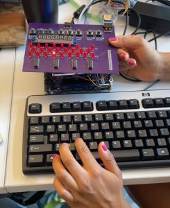
This week, I mainly worked with Tanisha on the layout of the PCB. We finalized some of the arrangement of the PCB (such as moving the buttons and rotary encoder to be above the 7 segment displays) as our parts started to come in and we could get a sense for how they would fit together on top of the FPGA. Once these decisions were finalized, we were able to start thinking about how best to format our silkscreen and other aesthetic choices so that users could easily use our product and for it to be more historically accurate.

Above is our most recent PCB layout, with a single rotary encoder on top, 8 buttons to control the 8 seven segment displays, and the display underneath it. The microSD card reader pins are to the right and the lampboard is underneath the buttons. There are four shift registers to cover the many outputs of the lampboard, and the DE10 header is on the bottom right.

Additionally, Amelia and I met to discuss the plan moving forward on the RTL now that she had successfully implemented the PS/2 protocol. She also caught me up on what I had missed when I was sick on Wednesday, and we had our ethics discussion as a team after that. We decided that the most pressing issue after the PS/2 was to ensure that the microSD card protocol worked as well.

However, after the issues we had with our PS/2 keyboard (see the team status report), I started to worry that we may have the same problem with our microSD card reader, since it requires 5V. While there is a 5V source pin on the FPGA GPIO header, all of the GPIO pins are 3.3V logic, and we do not want to provide too much voltage to the pins. After looking at the Amazon reviews and description of the microSD card reader, it still seemed ambiguous if it could function with both 3.3V and 5V, as the reader does step down the 5V to 3.3V internally. I plan on testing the reader now that it has been delivered to see what the idle voltage of the MISO line is, and hopefully it is 3.3V. Otherwise, we may have to explore other ways to regulate the voltage.

Next week, I will focus on the microSD card functionality. This includes verifying that the reader will work with 3.3V so that we can finalize this on our PCB, and then I will move onto implementing SPI protocol for the microSD card in RTL. Our PCB is moving along nicely, and I will help Tanisha with the traces as needed. Overall, we are on track, especially since the keyboard issue resolved itself with Amelia’s hard work!

Nancy’s Status Report for 3/8

Since the last status report, I mainly worked with Amelia on completing a lot of the writing for the design report. I specifically worked on the use-case requirements, design trade studies, the system implementation for the custom PCB, the test and validation, and the risk management.

Additionally, when finalizing the components on our PCB with Tanisha, we realized that a matrix scanning implementation of the keyboard would be overly complicated and would require many GPIO pins. I spent some time researching alternatives to keyboards, since we did not want to implement a complicated USB protocol for a USB wired keyboard. When doing more research, I found that the Altera DE10-Standard had a PS/2 port which would support a PS/2 keyboard with a much simpler protocol, so we pivoted our design back to the DE10, which allowed for one PCB that will fit on the top of the DE10. This is also what I wrote about in the design trade studies section of our report.

We initially hoped to have our PCB out for fabrication before spring break, but due to our last minute changes in design and FPGA type, this will be delayed. I will work with Tanisha on the layout this week so we can have it ordered by this week. While we wait for the PCB to be delivered, I will also work with Amelia on the RTL so that we are not wasting time, which will catch us back up to schedule. I hope to complete the PCB layout by this week and start on the implementation of some of the RTL modules.

Nancy’s Status Report for 2/22

In the beginning of the week, I finalized the design presentation, especially making sure that our use case requirements were quantifiable and translated into quantifiable design requirements. Later, I worked on the design report, adding more to the introduction and use case requirements sections. Most of this was elaborating on how our use case and its social/economic/historical implications leads to our quantitative requirements.

I also worked with Tanisha on finalizing our PCB schematic. While reading the De0-Nano datasheet, I saw that we had overlooked how the ADC pins are on the bottom of the FPGA, unlike the 2 2×20 GPIO pins. However, the ADC pins are also only accompanied by 13 GPIO pins, so it would not be possible to put all of our I/O on the bottom pins. So, I began exploring how to split up our PCB into 2, with the rotor functionality on the bottom pins where the potentiometers would be (which would need the ADC pins), and the lampboard/SD card/keyboard using the top pins. Additionally, I spent some time looking for the footprint for the FPGA, but I could only find a Fusion-compatible version for the bottom pins. This was a concern since we wanted the PCB to fit perfectly over the top pins on the FPGA and we want the spacing between the two 2×20 headers to be accurate. However, since we can move some functionality to the bottom pins, we only have to use one of the 2×20 headers, eliminating this concern.

Finally, I also researched into interfacing with the ADC and SD card reader through the FPGA. I found two Intel IP cores that work with Quartus that could be helpful — the ADC and SPI cores.

In order to stay on schedule, Tanisha and I need to finalize the PCB schematic and layout before spring break, which will be a good amount of work but doable with us both. This week, I hope to finish this so we can order the PCB over break, and also continue to edit the design report once we receive feedback on our presentation.