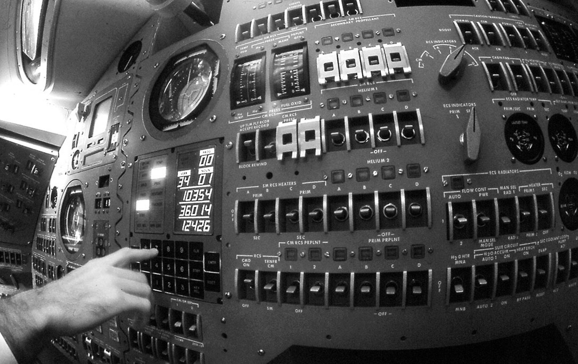
Given that we have settled on using an Altera DE10-Standard dev board to implement the core components of our system, I located its PDF Manual from the Altera website and made a few high-level notes. This particular dev board has a Cyclone V System-On-Chip (SOC) that includes both an FPGA and an ARM core to run embedded C programs. I confirmed with Jae that the included GPIO will be sufficient to interface with the DSKY. I’ve discovered that we’ll need to check our current versions of Quartus and possibly add additional software packages that allow us to write programs and then run them on the included core. Assuming that we go forward with writing a program that feeds simulated sensor data to our CPU on the FPGA, we’ll need to get familiar with the Advanced eXtensible Interface (AXI) bridge included on the Cyclone V as an interface between the FPGA and core, and I plan to personally do just that in the coming week.
Our current plan specifies the use of Altera’s ‘altsyncram’ megafunction IP to implement our dual-ported RAM and single-ported ROM. I’ve been reading through the Altera Manual in the efforts of learning how we will use Quartus to generate the modules we need. The included parameter table has allowed me to make note of exactly how we will configure each parameter to produce the desired functionality of our memory modules. I plan to finish making note of these in the next few days.
Christopher generated the core structure of our Architecture in schematic form, but I’ve been looking back at our detailed ISA notes to make subtle changes that will permit us to process all of our desired instructions. These changes have involved re-routing various nets to ensure correctness with pipeline stages as well as adding additional control signals. Through discussion, we’ve realized that a subset of double word instructions can be added to our scope with little implementation difficulty, so I will be working on ensuring correctness of our architecture for these additional instructions.
