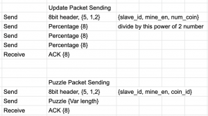
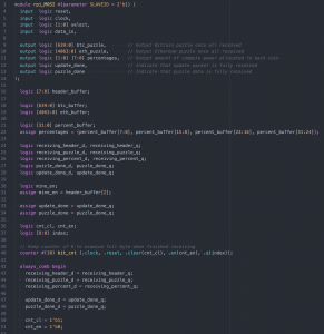
As mentioned last week, I wanted to more fully flesh out the communication modules. I was able to accomplish this and catch up with my assigned tasks such that I am now on schedule to complete my portion of the work. This week I worked further on the top and communication SystemVerilog files. Seeing as our FPGAs arrived but the Raspberry Pi was still being delivered, I focused my attention on developing the FPGA files instead. I added combinational logic for both input communication and output communication to the FPGA. This controls whether the FPGA is receiving a parameter update packet or a crypto mining packet.

The modules that I added are now capable of handling both MOSI and MISO communications. The specifications for the two were different so two modules were needed for both. It includes combinational logic to control which buffers to write to along with sequential logic that determines which state the module is currently in.

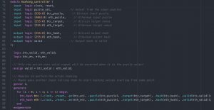
I also started working on the hashing controller for the FPGA. I researched the hashing algorithms for the cryptocurrencies we are planning on using and added module interfaces for those algorithms. I plan to decrease the wire sizes of the input puzzles in order to reduce the board area size taken by the controller.

I am on schedule to complete my tasks in time for testing before Spring Break. There is about one to two weeks of work left on the FPGA files before I will run them with a testbench through VCS simulation. Additionally, I plan to synthesize and test it on the board as well. In the next week, I plan to solidify some of the more subtle details of the code such as wire sizes and number of hashing modules in order for the code to be ready for testing. With the arrival of the Raspberry Pi next week, I will also pivot towards developing software code for the RPI.
