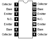
| Collector-Base Voltage, VCBO | 60V |
| Collector-Emitter Voltage, VCEO | 30V |
| Emitter-Base Voltage, VEBO | 5V |
| Continuous Collector Current, IC | 500mA |
| Total Device Dissipation (TA = +25°C, Each Transistor), PD | 0.65W |
| Derate Above 25°C | 5.2mW/°C |
| Total Device Dissipation (TA = +25°C, Total Device), PD | 1.9W |
| Derate Above 25°C | 15.2mW/°C |
| Operating Junction Temperature Range, TJ | -65° to +200°C |
| Storage Temperature Range, Tstg | -65° to +200°C |
Electrical Characteristics: (TA = +25°C unless otherwise specified)
| Parameter | Symbol | Test Conditions | Min | Typ | Max | Unit |
| OFF Characteristics | ||||||
| Collector-Emitter Breakdown Voltage | V(BR)CEO | IC = 10mA, IB = 0, Note 1 | 40 | - | - | V |
| Collector-Base Breakdown Voltage | V(BR)CBO | IC = 10µA, IC = 0 | 60 | - | - | V |
| Emitter-Base Breakdown Voltage | V(BR)EBO | IE = 10µA, IE = 0 | 5 | - | - | V |
| Collector Cutoff Current | ICBO | VCB = 50V, IE = 0 | - | - | 50 | nA |
| Emitter Cutoff Current | IEBO | VEB = 3V, IE = 0 | - | - | 50 | nA |
| ON Characteristics | ||||||
| DC Current Gain | hFE | VCE = 10V, IC = 10mA, Note 1 | 75 | - | - | |
| VCE = 10V, IC = 150mA, Note 1 | 100 | - | - | |||
| VCE = 10V, IC = 300mA, Note 1 | 30 | - | - | |||
| Collector-Emitter Saturation Voltage | VCE(sat) | IC = 150mA, IB = 15mA | - | - | 0.4 | V |
| IC = 300mA, IB = 30mA | - | - | 1.6 | V | ||
| Small-Signal Characteristics | ||||||
| Current Gain-Bandwidth Product | fT | VCE = 20V, IC = 20mA, f = 100MHz, Note 1 | 200 | 350 | - | MHz |
| Output Capacitance | Cobo | VBE = 19V, IE = 0, f = 1MHz | - | 4.5 | 8.0 | pF |
| Input Capacitance | Cibo | VBE = 0.5V, IC = 0, f = 1MHz | - | 17 | 30 | pF |
| Switching Characteristics | ||||||
| Turn-On Time | ton | VCC = 30V, VBE(off) = 0.5V, IC = 150mA, IB1 = 15mA | - | 25 | - | ns |
| Turn-Off Time | toff | VCC = 30V, IC = 150mA, IB1 = IB2 = 15mA | - | 250 | - | ns |
| Note 1. | Pulse test: Pulse Width </= 300µs, Duty Cycle </= 2%. |
 Home
Index
Back