Due Wednesday October 7, 1998
Note: this homework has a lot more detail than the typical review-style homework questions used in this course; but it has proven to be the only effective way to get the concepts across. This assignment was a lab in the previous incarnation of this material, but in this course the lab answers are provided, so you just have to answer the questions. If you want to do the lab work as well for your own enlightenment, everything you need is at /afs/ece/class/ece548/www/hw/hw5
You have signed on for an embedded system design effort that will be using the Samsung ASIC 0.5um STDL80 Library. You have been assigned to perform the design tradeoffs for an on-chip L1 cache using a 64-bit processor core. You're going to use their STDL80 memory compiler, and for this homework will use their documentation for your tradeoffs. The data sheet you'll need is in a file for your convenience. If you must go from hard copy, please save a tree and print only the pages indicated in the problem descriptions below -- note that the pdf viewer "page number" doesn't exactly correspond to the page numbers in the image file which are used in this assignment.
Because you're on a tight space budget to keep the chip inexpensive, you'll only have room for 2 KB of L1 cache on-chip. Also, this is a preliminary design exercise, so you're going to have to settle for using miss rate and traffic ratio from Dinero simulations to make your decisions. Fortunately for you, your boss is utterly convinced if you perform well on the spice trace from the H&P book collection your chip will be a success, so you only need to optimize for this one program (and, even more fortunately, he's already run all the Dinero experiments for you).
Terminology note: Cragon terminology (sector+block) is used in this homework unless specifically prefixed with the word "dinero". Remember that a Dinero "block" is a Cragon sector, and Dinero "sub-block" is a Cragon block. In some places this is re-emphasized for clarity.
Start your design effort with an evaluation of a unified cache. Use the dual-ported memory on pages 5-38 to 5-46 of the Samsung RAM generator document so that the processor has enough bandwidth available access both an instruction and a data word on each clock cycle. Be sure to note the Ymux range restrictions on page 5-38.
The output of dinero simulations is in the table and graph below for the Spice trace file using 2 blocks per sector (use sub-block placement in dinero, so this means 2 dinero "sub-blocks" per dinero "block"), direct-mapped, demand fetch, write-through, write-no-allocate. Word size and bus size are both 32 bits (the CPU uses a segmentation register scheme to address beyond 32 bits). The cache will contain 2 KB of data plus space for tags and control bits, all stored in a single memory array. Your system will employ a 53-bit, byte-addressed virtual address space and a 41-bit, byte-addressed physical address space with a physically addressed cache. It is a uniprocessor, so no "shared" bit will be needed in the cache.
| Block Size | Unified Miss Ratio | Unified Traffic Ratio | Split Miss Ratio | Split Traffic Ratio |
| 4 | 0.3114 | 0.3455 | 0.3354 | 0.3834 |
| 8 | 0.2165 | 0.4366 | 0.2168 | 0.4566 |
| 16 | 0.1743 | 0.6416 | 0.1572 | 0.6085 |
| 32 | 0.1557 | 1.0487 | 0.1273 | 0.9118 |
| 64 | 0.1507 | 1.929 | 0.1144 | 1.5314 |
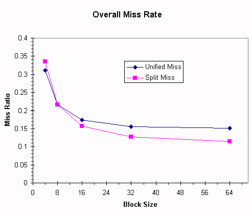
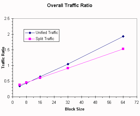
These data may be a slight surprise; apparently there are conflict misses between data and instructions in the direct-mapped cache, and separating them into a split cache reduces these conflicts.
Problem 1:
1. Based on the above results, you decide to pick a block size of 16 bytes (a Cragon block size, which is dinero "sub-block" size). Note that with respect to the memory array being used to construct the cache, an array "word" has nothing to do with the machine word size. Instead, an array word size is the number of bits accessed simultaneously from the array. For your design, a memory array word will contain exactly one sector -- data, tag, and control bits. How big is this memory array word (in bits)? How many of these words are in the cache memory array?
2. Although it may not be entirely obvious in the documentation, the Ymux design parameter indicates how many user-visible words are placed on the same memory array row. Thus, for Ymux of 4 there are 4 cache sectors on each memory row (i.e., 4 memory "words" per row). Draw a picture similar to the ones used in class to indicate a physical layout of a memory array with Ymux values of 4, which would have 4 cache sets in each memory row. You may elide some of the rows similar to what is done in cache pictures used in the lecture notes as long as the number of rows is clearly labelled. (Assume that a single memory array can hold all the bits for each set in order to keep the picture simple.)
3. The table on page 5-38 indicates limitations on the number of bits that can be in a memory word (each memory word equals one set having one sector in our example case). So, you will implement the cache by splitting the bits among several equal-size memory arrays (e.g., to get an effective memory word of 64 bits with YMUX=16 you'd use 4 memory arrays -- the first memory array would have bits 0:15 and the last memory array would have bits 48:63 of the 64-bit memory word; round array size up to the nearest bit so all arrays are the same size, even if you throw a few bits away because of this simply to make the problem a little easier to work). Using the table on page 5-42 of the documentation, pick the Ymux type that gives the fastest access time (tacc) for the 16 byte block case. List the 5 values of tacc for the 5 Ymux types, and circle the lowest value. Assume fanout of 4 standard loads, input slope ("rise time") of 1 ns, and a cycle time of 50 MHz.
4. You try to synthesize the memory and find out that all cases except Y=2 are broken due to a software bug in the compiler, so you have to go with Y=2. How large is the total memory size (all arrays combined) in square microns?
Problem 2:
1. Now see if using a split cache is a win. Use the single-ported memory on pages 5-15 to 5-21 of the Samsung RAM generator document. Use a design process similar to that described in Problem 1 and the same cache operating parameters fed to dinero, except for a split cache system with 1KB each for I-cache and D-cache. Use the "1-bank" design option, not the 2-bank option (i.e., the design parameter ba=1) for the RAM generator calculations.
Just for the sake of discussion (and to save you the tedium of doing all those calculations for the split cache case), compute the total size of the split memory arrays for the same cache parameters as problem 1 part 3 above even though the tradeoff for performance might dictate slightly different parameters. Note that the number of memory words in each array will not be the same. Also the data size will be 1KB each for two split arrays instead of 2 KB of data for one unified cache. What is the total size difference in square microns using split single-ported RAM compared to the previous unified dual-ported RAM result -- which is bigger and by how many square microns?
Hint: You are supposed to use a split cache with the same total cache size (1 KB + 1 KB = 2KB total), so you'll need one more bit in each tag. This extra tag bit means you have to increase the number of bits in your memory array. So when you're doing the split cache size calculations you'll have to adjust the Bpw parameter accordingly.
Problem 3:
1. Your design team is going over its power budget, and you're getting pressure to reduce the power consumed by the cache memory rather than (necessarily) the area or speed. Perform a representative calculation on the single-ported memory on pages 5-15 to 5-21 of the Samsung RAM generator document. What is the normal mode (power_ck) power consumed for a Ymux value of 4, W=128, B=48, 3.3 Volt operation, and an operating frequency (F) of 33 MHz? What is the power savings of cutting the cache size in half by providing only 64 words? What is the power savings of keeping the cache size at 128 words, but instead reducing the voltage to 3 Volts? Note that for this question you are not using the same memory array size as for the previous problems -- it is merely a representative calculation of the type you would perform on the "back of an envelope" to get a feel for the design space.
18-548/15-548 home page.