Jose’s Status Report for 03/07

I spent most of the week working on testing out and debugging the FPGA interface with the built-in codec (apart from working on the design report with my team). There was some time spent getting caught up again on Quartus’ features and tools, since most of my recent work had been through the use of Vivado. Once that was over, I set up all the pin assignments as required for the I2C and I2S interface, being left with the following physical debugging setup:

The most significant 4 LEDs are meant to represent the state for the main I2C setup FSM, which is a four bit value. The next four are of the same type, but they show the states for the internal I2C protocol FSM (just to be clear, the main I2C setup FSM sends out the write commands while the internal one manages the actual ack handling, SDA pulling, etc.). Finally, the last two LEDs are meant to represent the error signal (in the case that something with the protocol went wrong) and the done_sending signal (which indicates that data finished sending). I spent a while trying to debug an issue with the overall setup FSM, wherein I was setting the “send_data” signal to high for only one clock cycle. This caused issues with the protocol FSM, because I have it set up so that it sends out data and manipulates the clock at a rate of 250 Khz (in the case of the 50Mhz clock, I’d be manipulating state once every 250 ticks). This caused “send_data” to not be perceived by the protocol FSM, and leave the setup FSM in its first state as the protocol wouldn’t be activated. Once I modified the setup FSM, the FPGA’s LED representing “done_setup” lit up. While this was the main factor for identifying that the system was functioning properly, it also helped that the CODEC began outputting audio from the line out port, as seen in the video below:

https://youtube.com/shorts/HG-n8KKO8Xg?feature=share

While I have a simple square wave being outputted, my plan for the next week is to more thoroughly test the audio CODEC and investigate how to extract its output for signal comparison in MATLAB. Specifically, I’ll try testing different types of audio output to see if there is variance with the output (that is, I’m not just outputting random noise). I’ll also look into using Quartus IP for generating a 12.288MHz clock utilizing a PLL (since right now my approach could most definitely be fine-tuned). This is in line with the schedule, and no catching up is needed.

Team Status Report for 03/07

So far, no changes to our schedule have been made nor new risks have been posed. Because the audio output system interface was set up with a square wave (or noise, it’ll be properly tested this following week), there is now a bridge into getting different signals outputted (and proper testing of waveform/filters). Right now, getting the CODEC functioning properly is the main priority and risk, but at the current pace we’re at it does not seem to pose too much of a challenge. Apart from working on the design report as a team, that is the main progress of the week. The video for the FPGA outputting audio can be seen in Jose’s status report.

How will our project meet the specific needs with regard to the following?

NOTE: A was written by Jose, B was written by Mihail, and C was written by Jose.

A (global factors):

In contrast to software synthesizers, hardware synthesizers are meant to be used without external computers or software. This means that FPGSZR can become much more accessible globally, since anyone can use it if they have a computer, no computer, or a variety of musical equipment. In other words, this means that people of all backgrounds can create music on a global scale (no matter the background, anyone can use the tool).  Thanks to the product’s ease of use and low cost, classrooms can integrate them into their coursework and have students learn about the fundamentals of digital synthesis.  Moreover, FPGSRZ’s standalone nature avoids any stalling thanks to external tools or instruments. That means that the system is reliable in many sorts of situations in which constant operation is required (live performances, classrooms, etc.).  Altogether, these factors identify how FPGSRZ can affect the entire world in a positive manner, not just being limited to the city of Pittsburgh or one cultural group.

B (cultural factors):

This project carries significant cultural impact due to the fact that it is meant to be a cheaper alternative to a musical instrument. Music is a key part of cultural expression, and access to instruments can affect who is able to participate in music production and creative communities. Traditional hardware synthesizers can cost hundreds of dollars, which may limit access for students, hobbyists, or musicians, especially those from lower income backgrounds. By designing a lower-cost FPGA synthesizer that still supports standard MIDI keyboards, polyphonic playback, and a wide range of effects such as filtering, reverb, distortion, and multi-band compression, our system helps lower the barrier to entry for electronic music creation. This accessibility allows individuals from diverse cultural and economic backgrounds to experiment with music creation and express their own musical traditions or styles. Additionally, because the system is modular and based on widely used standards such as MIDI, it can integrate with a variety of instruments and musical workflows used across different communities, supporting a more inclusive range of musical practices.

C (environmental factors):

This project carries a significant benefit to the environment thanks to the fact that we are using an FPGA as the center of computation. Traditional hardware synthesizers carry a multitude of specially made components that cannot be reused elsewhere (think integrated circuits and the like). When the devices serve their purpose, people are inclined to then throw it out and create technological waste. If disposed of improperly (which can occur often), toxic substances like lead and cadmium can be released. Because of FPGA’s reprogrammable nature, the user can reprogram its internals to serve other uses when they do not need to use a synthesizer anymore. Essentially, they can reuse the component and avoid the need of throwing anything out and creating e-waste. To us, this is the most significant environmental benefit that comes about from our project.

Team Status Report for 02/21

For this week, no particular changes were made to the overall design structure. Although we’ve spent the week working on specific portions of the design, nothing has caused the aforementioned or a change in our schedule. The biggest risk so far has to do with the audio codec, since it’ll be the main mechanism for testing our signal generation/effects in every possible way. If not finished on time (for this week), then the plan would be to spend time on spring break remediating any issues with it. This’d involve debugging through simulation and waveform analysis, checking with oscilloscopes as well.

Jose’s Status Report for 02/21

I spent this week working on the design/code for the FPGA’s audio codec. The following is split into two portions. The first has to do with the I2C protocol/wires that communicate with the CODEC. It’s impossible to ignore since it’s what needs to be utilized to send out the reset/power/setup write commands. With that in mind, I designed two handshaking FSMs for the purposes of 1. Sending out write commands for initializing the CODEC and 2. Handling the I2C protocol itself (i.e., sending out all the bits of data properly). The design for such FSMs can be seen below:

  1. I2C Protocol

This takes care to respect the I2C rules, particularly modifying the clock (which we provide) carefully when initiating data transfer. Just to note, the design also takes care of the fact that we’re transferring data at 100Khz (while the FPGA’s provided clock is going at 50Mhz).

2. Sending out commands

While the register we’re writing to is the same for all of these (address 0x34), the commands being sent all have unique hex values.

This was coupled with the actual interface with the CODEC, which was much simpler to implement since, apart from feeding the necessary clocks, data transfer is done through a parallel shift register.

This leads to an overall interface that looks like so:

Once all of that was done, I focused on setting up Quartus on my laptop for actually putting the code onto the FPGA and begin testing. While arduous, I got the pins set up and the entire system set to begin doing the previously described work next week. 

My progress is on schedule, as I’d marked this week for developing the initial design/code for the system and next week for debugging/testing the code as necessary. With that in mind, I hope to get a system in which some sort of audible noise is heard next week implemented on the FPGA itself (now that my Quartus is set up properly).

Team Status Report for 02/14

No changes were made to the overall design this week, and so far there are no significant risks involved with the project. As a team, we worked on getting the design proposal presentation ready, which included adding specifications for design requirements and the like. While our testing and solution methodology did not change, we were able to expand on the ideas we were establishing last week (one significant one was fixed-point representation for our signals, allowing for low latency and faster calculations over floating point operations). Our overall schedule has not changed apart from José’s focus beginning with audio output first and then going to MIDI interfacing (swapping the order). Here is an overview of the updated schedule:

A was written by Mihail Alexandrov

B was written by José Cestero

C was written by Kaloyan Stefanov

Part A:
The FPGA synthesizer processes all data digitally on a single device, avoiding high-voltage analog circuitry and therefore reducing the risk of electrical shock to users. This, along with prolonged exposure to high intensity audio output, are the two main health considerations in the project. We’ve discussed controlling output audio amplitude as a solution to the second issue. In terms of safety, the synthesizer operates at the low voltages characteristic of FPGAs and provides deterministic behavior due to the digital architecture, limiting failure points and reducing the likelihood of unexpected faults that could lead to safety risks. With respect to welfare, the project promotes accessibility to music creation by providing a lower cost, reconfigurable alternative to traditional synthesizers that could be adapted for both learning environments and creative expression.

Part B:

Our FPGA synthesizer will be made to take in input from an external MIDI keyboard, yet its internals will be made in a way such that all the processing is done on one singular component. This means that the external input device can be modified as we wish (while the internals stay the same), meaning that those who are impaired could use musical devices in ways that they normally could not. It expands the range of people who can produce digital music (and even invites the opportunity of having more disabled artists in the music space). This, moreover, relates to the fact that the device is meant to be low-cost and reproducible. While this relates to its economic factors, it also has to do with the fact that simply more people can express their cultures through music without any barriers. It all results in a long-run effect of democratization of musical production, such that musical communities become larger and cultural representation is broadened.

Part C:

Our FPGA synthesizer is aimed to be low-cost, providing a hardware alternative for those interested in electronic music but lacking the means to acquire a hardware synthesizer. By relying on an FPGA, we also provide users with ability to create modifications and improve upon the existing design. This makes the synthesizer even more economically viable, as we can provide updates to the actual design as development continues, providing users with a continuously improving product. In comparison, analog synths lack this reprogramming, making it difficult (if not impossible) to change the product once it’s been released. Indeed, one can envision an FPGA “music box” which can be configured in a multitude of different ways (guitar pedals, audio effect rack, etc.), a much cheaper hardware alternative compared to buying all these analog devices.

Jose’s Status Report for 02/14

This week I focused on primarily two things (apart from the design presentation, of course). The first was designing a system for receiving data from the MIDI shield, while the other was beginning to investigate how we’d get audio to output through the use of the DE10-Standard’s builtin 24bit CODEC. 

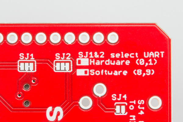
Regarding the first, I was investigating how the SparkFun MIDI shield outputted data being processed from the MIDI DIN cable.Serial Selection Jumpers

The board features the opportunity to select between hardware and software UART. For the purposes of the actual FPGA, we’re interested in selecting hardware UART (which is enabled by default). Software UART, however, is going to be useful when debugging how the FPGA is processing inputs, since further research revealed that connecting it to an Arduino would allow us to use the library developed by SparkFun to see how input should be properly interpreted (using Serial.print()). 

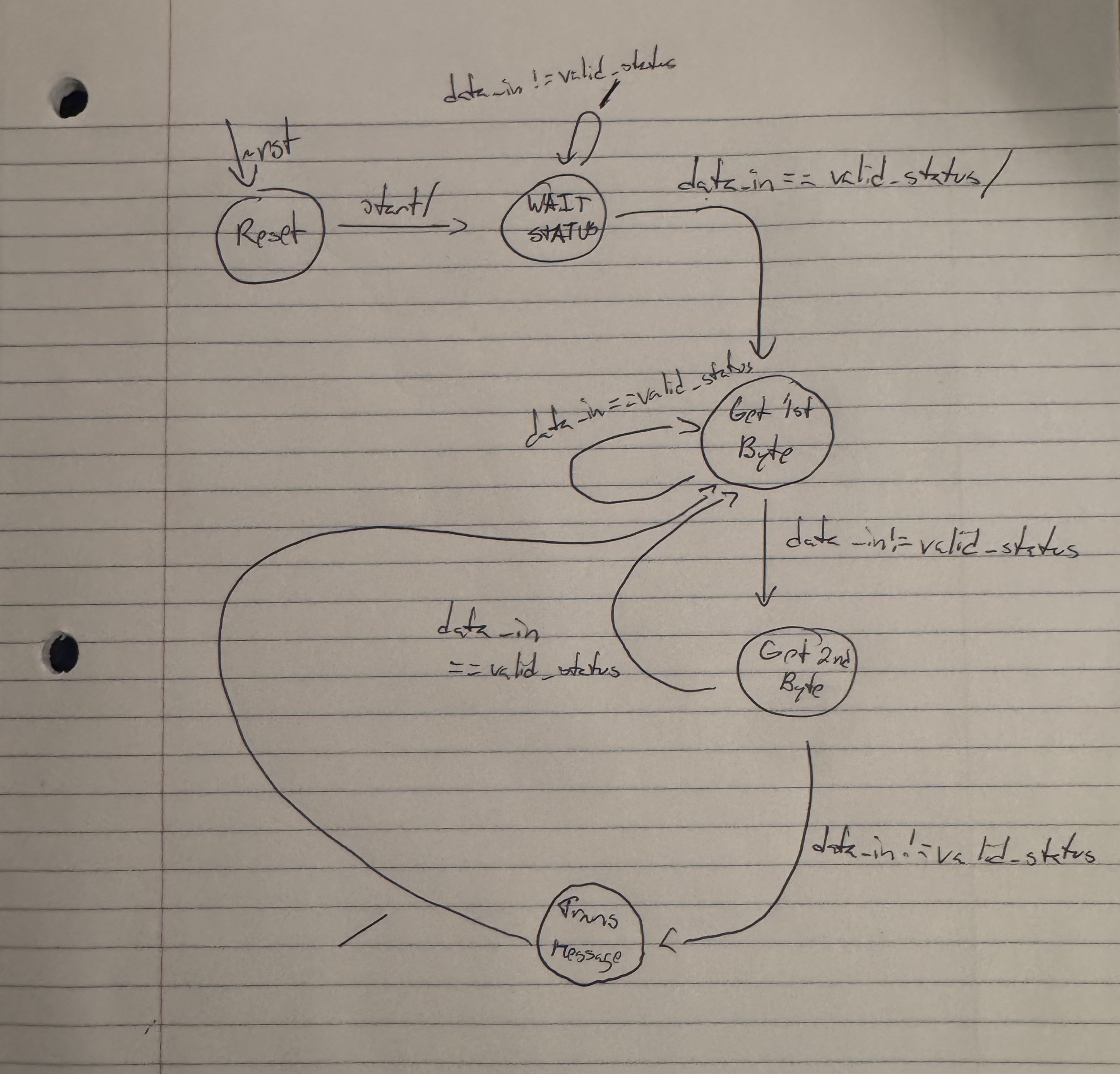
With this in mind, I knew that the hardware UART configuration would output data utilizing the standard MIDI message format as outlined here: https://www.songstuff.com/recording/article/midi-message-format/. This led to me writing up an FSM for parsing MIDI data as outlined here:


This is primarily designed for status messages sent out by the controller that contain two bytes, which are:

0x80: Note ON

0x90: Note OFF

0xA0: Poly Pressure

0xB0: Control Change

0xE0: Pitch Blend

The FSM will be waiting until one of these status bits is sent, storing it in a register and then transitioning to waiting on the two information bytes. If, at any point, a valid status byte is sent out, we transition back into waiting on the 1st byte. Once two data bytes are sent out, we transition into the TRANS_MESSAGE state (where the actual command will get transmitted onto the FPGA). This leads us going back into the GET_1ST_BYTE state, repeating the process all over again. This is a high level representation of what I’ll be trying to implement soon, so the design can (and will probably) be tweaked as needed.

After this, I began researching how the DE10-Standard’s audio codec worked. It supports 24-bit audio, utilizing a 2s complement format. Interfacing with it would require dealing with its I2S interface, utilizing a parallel-to-serial shift register (shifting out bit values one at a time). As I was going over the design for this and the MIDI interface, I realized that the most important baseline for setting up the project is the audio. My partners need a way to test out that their initial implementations are working properly, which means that I should focus on this first. While I’m still on schedule, I hope to complete a functional audio interface with the FPGA next week and then work on the MIDI interfacing afterward (essentially swapping the schedule for both tasks). Overall, though, I have a solid idea on how to move forward with implementing the designs for both.

Mihail’s Status Report for 02/07

This week I worked with my teammates on the project proposal presentation. In particular, I assessed requirements for the audio quality, such as determining latency and SNR thresholds. I also came up with guidelines for testing, and worked directly with my other teammates to put in the product orders for the project. Next week, I hope to continue planning out the project for the design presentation, particularly to focus on the block diagrams / hardware design for audio processing inside of the FPGA.

Team Status Report for 02/07

The team worked together this week discussing project requirements and whether some goals (drum playback) were too ambitious for the project. Overall, we determined that we’d keep the goals as is, since initial research from everyone revealed that some goals (like MIDI keyboard input) could possibly be completed earlier, allowing for some more leeway in the case that things go wrong. While we have been discussing initial system drafts, our plan is to work on block diagrams next week for our high level vision of the design. This aligns with our schedule outlined in the gantt chart, such that no changes are envisioned. Our general proposal and set of features stays the same, and we’ve begun gathering the materials for the project (DE10 Standard FPGA and MIDI Keyboard) in order for us to kickstart both the design process and initial implementation steps next week. The biggest risk for blocking progress as of now seems to be our team’s lack of DSP experience. Learning some of the techniques and algorithms for filtering, then, could potentially cause us to spend more time on planning/designing some sections of the project. In the case that this happens, our plan would be to dedicate extra time (~3 hours a week) into reviewing content from 18-290 more in depth and implementing algorithms in simulators like Matlab in the case of confusion.

Kaloyan’s Status Report for 02/07

This week, I worked with my teammates on our proposal presentation. I designed the block diagram and solution approach, along with working out what audio effects we would implement and coming up with the idea for an additional drum track. For next week, I’m looking forward to working on the design presentation and figuring out the more technical aspects of the RTL, along with beginning to write the RTL for the wavetable generation.

Jose’s Status Report for 02/07

Most of my work this week involved researching what components I wished to use for the MIDI input interfacing with the FPGA and how I would get them to work together (at a high-level, of course). There were two main options for MIDI input, and that involved either using USB or the dedicated MIDI DIN cable to connect with the FPGA. My research yielded that these come with their own benefits/tradeoffs, being:

USB:

  1. High bandwidth (with a full speed of around 12Mbps)
  2. No external hardware necessary (meaning that the USB can directly interface with the FPGA)
  3. Non-deterministic timing (USB communication is based on sending packets of information, which may need to be polled at times)
  4. RTL necessary for interfacing would be much more complex, since I’d need to account for different channels, timing, and more complex state control

MIDI DIN:

  1. Lower bandwidth (a full speed of ~3.1kB/s)
  2. External hardware necessary (ideally, can just use a MIDI breakout board)
  3. Deterministic timing
  4. RTL necessary would be much simpler (since DIN MIDI is byte-serial and self-clocking, meaning that error handling is less complex)

With all this in mind, I chose to approach interfacing on the FPGA through the use of MIDI DIN. My logic for such was that the interface will be pivotal for testing all the wave generation and sampling we produce, so going with the simpler option would allow for us to begin testing as early as possible and better guarantee that we have some sort of working product on time. Moreover, if I can save time on interfacing, that means that I could spend more time on working on filters and adding drum sampling features later on.

Once I decided on using MIDI DIN, the next step was beginning to figure out what keyboard I’d use (that had that output port type) and how I’d properly interface with it/the FPGA. I ended up picking the following keyboard:

Amazon.com: Monoprice 606607 MIDI Keyboard Controller - Black, 49 Key | Pitch-bend & Modulation wheels, Driverless plug and play for Windows and Mac PCs - Stage Right Series : Musical Instruments

This is the MONOPRICE 49-Key MIDI Keyboard Controller, which has enough physical buttons and features to implement the functions we want to. Moreover, it contains both USB and MIDI DIN output (in the worst case where I decide on pivoting back to USB output). Because this was available on the ECE Parts Inventory, it was also a wise decision since it allowed us to save on budget for other expenses, like the MIDI DIN breakout board.

There were many options for what I could use when interfacing with the keyboard, but my research ended up pointing to the SparkFun 12898 MIDI Shield:

MIDI Shield Arduino R3 Shield Project Kit

This component, while being in stock on DigiKey, has detailed documentation for processing input/output. Apart from that, it has deterministic output, making parsing key data much less complicated. The other option would have involved assembling a decupler circuit (either using a PCB or physical board, which would likely create complications further if physical failure needed to be debugged). This leaves the high-level interaction between the keyboard and FPGA much clearer, since it’d involve connecting the keyboard to the MIDI shield, and then have the shield communicate with the FPGA. We’d just need to solder the connections, which is not complicated.


Overall, I feel like I did good progress researching this week, and am left with a clear direction on what to keep pursuing next week. Now that we have an FPGA from inventory, my plan is to begin developing the VGA interface on hardware and start developing code for parsing output from the MIDI shield (which will be ordered soon). I can say that everything is on track, and no time has been wasted.