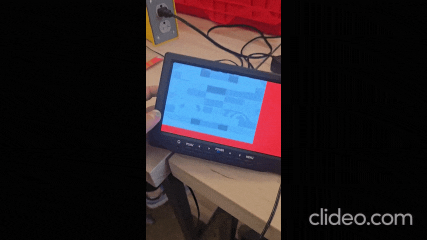
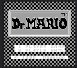
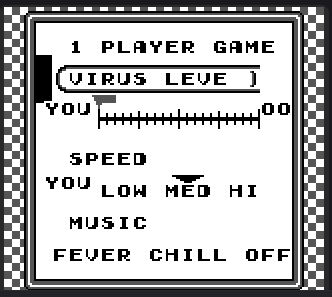
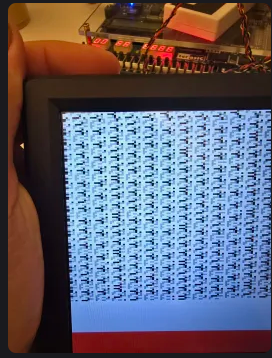
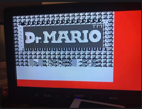
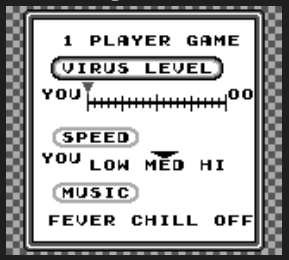
Team Status Report 2/8/25

Progress:

  • CPU:
    • All frameworks completed.
    • Instruction buffer added.
    • Instructions implemented: 2
  • PPU
    • RTL completed based on datapath.
    • Testbench development in progress.
  • MMU
    • Re-designed memory controller to utilize FPGA Block RAMs instead of DE II SRAM/SDRAMs for simplicity of integration
    • Synthesized and tested Block Rams of different sizes (in ROM and RAM variant) and confirmed that they work
  • Other I/O
    • Did research into USB/Audio integration. Discovered that NIOS II cannot be used,  but there are IPs provided by Altera that use an Avalon master/slave interface.
Design Changes:
  • Swap to 32-bit word memory is under consideration.
  • Swapped memory units for BRAM

Risks and Risk Management:

  • If a swap to 32-bit words is confirmed, a full reworking of the instruction buffer will be required.
    • CPU will be developed with the assumption of 16-bit words until told otherwise since the 16-bit word architecture is harder to implement.
    • To make the possible transition easier, we will mark all code that must be removed or replaced if this change occurs.
  • Memory has been tested but I/O parts still need to be confirmed ASAP.

Ruslana’s Status Report for 2/8/25

  • Researched memory options on FPGA DE 2 board (block rams, SDRAM, SRAM, Flash) and explored options through Quartus Megawizard IP Interface
  • Discussed with Professor Nace for potential options on FPGA memory
  • Derived new design based on FPGA Block RAMs based on discussion with Bharathi and Katherine on CPU/PPU accesses
  • Re-designed Memory Controller Datapath to utilize block RAMS
  • Obtained DE II 115 boards from Quinn and distributed it to members
  • Created 5 generic memory modules for Block RAM
  • Created testbench for each memory module in simulation and Chip Interface
  • Synthesized and tested BROMs/BRAMs on FPGA and confirmed success by empirical validation
  • Did research into audio/USB integration and realized NIOS II is a soft-core processor that you can write C code for, but it gets synthesized onto the FPGA and uses up the LUTS. It’s a way to give people an easy route to write C code to be used on FPGA, but not on on-chip computer that talks to the FPGA itself.
    • FPGA University Program on Quartus ECE Machines gives some kind of Qsys interface to create USB and Audio IP devices? Requires further research.

Bharathi’s Status Report for 2/8/25

Accomplished

My goal for this week was to finish my datapath for the PPU and get the RTL complete so I can begin testing next week.

I have completed the RTL and verified that my code is synthesizable. I tested some of the smaller modules dedicated to sprite searching and pixel/frame buffering. I have already started working on the testbench which is my main task for next week. I also helped Ruslana with research into some FPGA memory use questions.

I also spent some time this week working on the slides for the design presentation and did some research into effectively mapping out some of our qualitative use-case requirements to more testable quantitative design requirements.

Schedule / Progress

As I have already started working on the testbench and I am also almost done with my design presentation slides, I think that should put me well ahead of schedule at the moment.

Next Step

My main goal for next week is to debug as many single-frame rendering cases as time allows. I’ve mapped out about 20 different edge cases across sprite priority, sprite search, FIFO and memory related operations that need to be tested.  I expect this round of testing to be somewhat involved because my testbench needs to be able to simulate everything — memory, CPU updates to control registers, interrupt handling etc.

I also plan to finish up any updates to my design presentation slides based on feedback and start preparing for the actual presentation.

Katherine’s Status Report for 2/8/25

Accomplished:

  • Proposal presentation thouroghly practiced and given.
  • CPU testbench framework made for ModelSim.
    • Tests can be easily added to the testbench.
    • Can pick which test to run from the terminal.
  • CPU basic framework completed.
    • ld r,n (load immediate) passes handmade tests.
    • ld r,r’ (move) passes handmade tests.
  • Instruction buffer implemented and passes handmade tests.
Next Step:
  • Implement all memory instructions.
  • Make handmade tests for all memory instructions.
Other Notes or Concerns:
  • Progress is slightly ahead of schedule.
  • Memory and control flow operations are being prioritized so the other units can be tested using ROMs