
- Not much to report because of finals work, but mostly:
- worked on capstone final presentation
- attempted to explore timer bug and found that modifying timer registers/system clock frequency had no effect
Ruslana’s Status Report for 4/19/25
Mostly all included in team update list.
- Debugging FPGA with the rest of team
- Learned how to use SignalTap to focus on probing CPU register values/Interrupt register values, but it’s been slow
- Resynthesizing design gives different behavior, which is worrying, but our design is also quite sensitive to change right now (we attempted to refactor to eliminate X’s and this caused some new frame artifacts to show up)
- Hoping to fix immediate issue with double speed and pill
Learned things:
- Learned about NIOS II processor and how complicated altera toolchain is
- Learned about signal tapping to debug on FPGA
- Learned about dealing with multiple clocks on design
- Learned from my partners about how to tackle large scale combinational loops in a pragmatic manner
- Learned about modelsim
- Learned about memory interfaces and communication protocols (to SDRAM, SRAM, Audio CODEC), though we haven’t been able to utilize it so much for our project
Most of this came from trial and error + scouring the internet.
Ruslana’s Status Report for 4/12/25
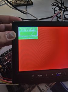
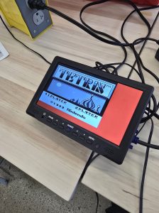
- Debugged Tetris and Dr. Mario based on the frames (see Katherine/Bharathi’s status reports for more detail)
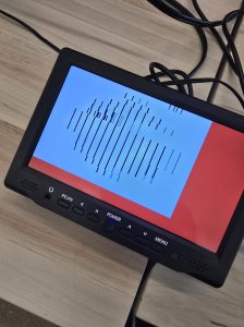
- Created frame buffer from BRAMs and used it to render vga frame (preinitialized with our tetris.ppm frame). Also upscaled it to support a larger display.
- Rendered dmg-acid-test with pure ROM, incorrect but not far off so we proceeded to start debugging entire design on FPGA.
- Wrote the APU (4 channels with envelope/sweep/volume/pseudorandom noise manipulation). Unsure if we will get to implement this.
- Did some research on the side and came up with a plan to use SDRAM and UART through raspberry pi to support MBC for games that have more memory than FPGA block rams can support (but it seems like we will not have time to do this)
- Currently debugging Dr. Mario ROM on fpga + vga setup. Using signal tap and slower clocks to step though the PCs and cross-comparing between simulation and synthesis to check.
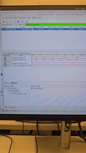
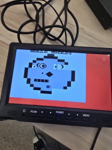
Some images throughout the week of the process (signal tap + vga/frame buffer timing bugs):
Ruslana’s Status Report for 3/29/25
Accomplished:
- Verified MMU and CPU are integrated with all except interrupt tests (which we are now working on, due to also adding the PPU)
- Integrated all units but APU
- Made a testbench to test full integration
- Started debugging all units with Tetris and dmg-acid-test
- Synthesized all units on Quartus. After catching some latches, we confirmed that it is indeed synthesizable. We are using the amount of memory that we expect, but surprisingly, there is low LUT usage. Hopefully, this is not an indication that stuff is being optimized away, but the Technology RTL Viewer on Quartus is showing all of the circuitry and fllip-flops for our 3 designs.

Next Step:
- Work on debugging Tetris
Other Notes or Concerns:
- We are on schedule.
- The blargg interrupt tests can’t be fully run due to timing optimizations done to the PPU. However, what was able to be run shows that interrupts will probably work.
- Most MMU bugs have been subtle address calculation problems or actual differing interpretations of spec details that are getting noticed with each test, but no enormous internal failures. It is servicing the PPU and CPU fine.
Ruslana’s Status Report for 3/22/25
- Timer/PPU/APU IO Registers work, in addition to BRAM modules in MMU!
- Currently (in between typing this report) debugging DMA functionality–MMU is almost completely testbenched enough for integration to be full sent
- First integration test between CPU/MMU has been written and compiled with a fresh Makefile and a basic tb has been created, and debugging more thoroughly is scheduled for tomorrow
Ruslana’s Status Report for 3/15/25
- Went through MMU code review with Katherine/Bharathi. Reevaluated some interrupt routine code and corrected it accordingly
- Created python script for acquiring .mif files when given a binary ROM obtained from online
- Created basic testbench for MMU to stress memory r/w, IO r/w routines.
- Testbenching MMU and verifying:
- basic memory cpu/ppu read/writes to all BRAMS(ROM, VRAM, EXRAM, WRAM, OAM, HRAM)
- basic cpu IO read/writes (timer registers, APU registers, PPU registers, interrupt registers)
- DMA transfer during hblank/vblank works without interfering with the above
- Currently, basic BRAM tests to each memory unit are good for all ppu modes.
- Currently waveforming and debugging IO integration (timer registers are working, still need to verify the rest)
Remarks:
I’m confident that integration can start by next week, because I am developing high confidence in the Memory Controller being ok-enough for talking to the CPU. The edge cases can be caught during actual execution. I caught a lot of erroneous behavior with my personal testbench, but it’s still a model of what I expect the communication to be based off on Pandocs, not the actual ROM’s behavior.
Ruslana’s Status Report for 3/8/25
Accomplishments:
- Finished writing first version of MMU and pushed to github.
- Created the block rams we intend to use for ROM banks and RAM units (VRAM, WRAM, External RAM, OAM table, HRAM)
- Wrote logic for all IO hardware registers
- Currently debugging MMU against a simple testbench to check bram read/writes and register read/writes
- Currently writing first version of APU to be pushed because of my current familiarity of the audio hardware registers from writing MMU
Goals for next week:
- Top priority is to complete testbenching MMU so that it is compatible for handoff to the CPU and PPU, this will take a some days from now but it’s looking up
- Begin testbenching APU afterwards
- NIOS II work put on hold for now, but I resolved the blocker from last time of unable to use the terminal tools on ece machines
Remarks:
Feeling a little bit tight on schedule with MMU because I spent too much time digging at other more exploratory forms of IO integration, but if I lock in for the next week, we should still be on track to hit MVP.
Ruslana’s Status Report for 2/22/25
- Spent a lot of time researching USB integration again
- Tore through Altera Memory Mapped Interfaces for Master/Slave, seems feasible to integrate with SRAM Controller. Less worried about that integration.
- Created several Altera MM modules that were able to be placed in Qsys Platform Designer, and routed to the SRAM controller and other interfaces
- Qsys (platform designer) allows individual IPs to be layed out along with Avalon IPs, and the interconnect logic gets automatically generated
- Looked through on chip Cypress USB Controller and realized it had to use NIOS II soft core cpu to communicate, other forms of communication would be our own version of writing a USB OTG Controller to interface with it
- All altera examples involved declaring the NIOS II soft core cpu on the FPGA (thereby using up LUT resources)
- And also writing USB driver code in C to support talk to the USB peripheral. This seemed tedious at first.
- After many hours of research for documentation, results on the doc were sparse. Although writing a custom RTL unit to communicate to Cypress doesn’t seem impossible, it would involve trial & error and a lot of stabbing at a black box.
Therefore, I’m pivoting to trying the Raspberryp Pi GPIO route as a back up plan, but also trying to synthesize part of the NIOS II soft core CPU. This may also enhance integration with the audio CODEC as well, because the Wolf chip has a similar problem.
Ruslana’s Status Report for 2/15/25
- Re-evaluated memory spec with Katherine and Bharathi
- Held a design review with Bharathi on her PPU implementation
- Re-worked DMA specification with Katherine and Bharathi and memory size of each Block RAM
- Learned more about Avalon slave interface to communicate with peripherals (SRAM, audio)
- Writing Memory Controller (with updated DMA, newly Quartus generated Block RAMs)
- Writing unit tests for USB/Audio –> will test by Sunday
Ruslana’s Status Report for 2/8/25
- Researched memory options on FPGA DE 2 board (block rams, SDRAM, SRAM, Flash) and explored options through Quartus Megawizard IP Interface
- Discussed with Professor Nace for potential options on FPGA memory
- Derived new design based on FPGA Block RAMs based on discussion with Bharathi and Katherine on CPU/PPU accesses
- Re-designed Memory Controller Datapath to utilize block RAMS
- Obtained DE II 115 boards from Quinn and distributed it to members
- Created 5 generic memory modules for Block RAM
- Created testbench for each memory module in simulation and Chip Interface
- Synthesized and tested BROMs/BRAMs on FPGA and confirmed success by empirical validation
- Did research into audio/USB integration and realized NIOS II is a soft-core processor that you can write C code for, but it gets synthesized onto the FPGA and uses up the LUTS. It’s a way to give people an easy route to write C code to be used on FPGA, but not on on-chip computer that talks to the FPGA itself.
- FPGA University Program on Quartus ECE Machines gives some kind of Qsys interface to create USB and Audio IP devices? Requires further research.