Bharathi’s Status Report for 2/22/25

Accomplished

My goal for this week was to debug the PPU and scope out what updates would be necessary for the full color implementation.

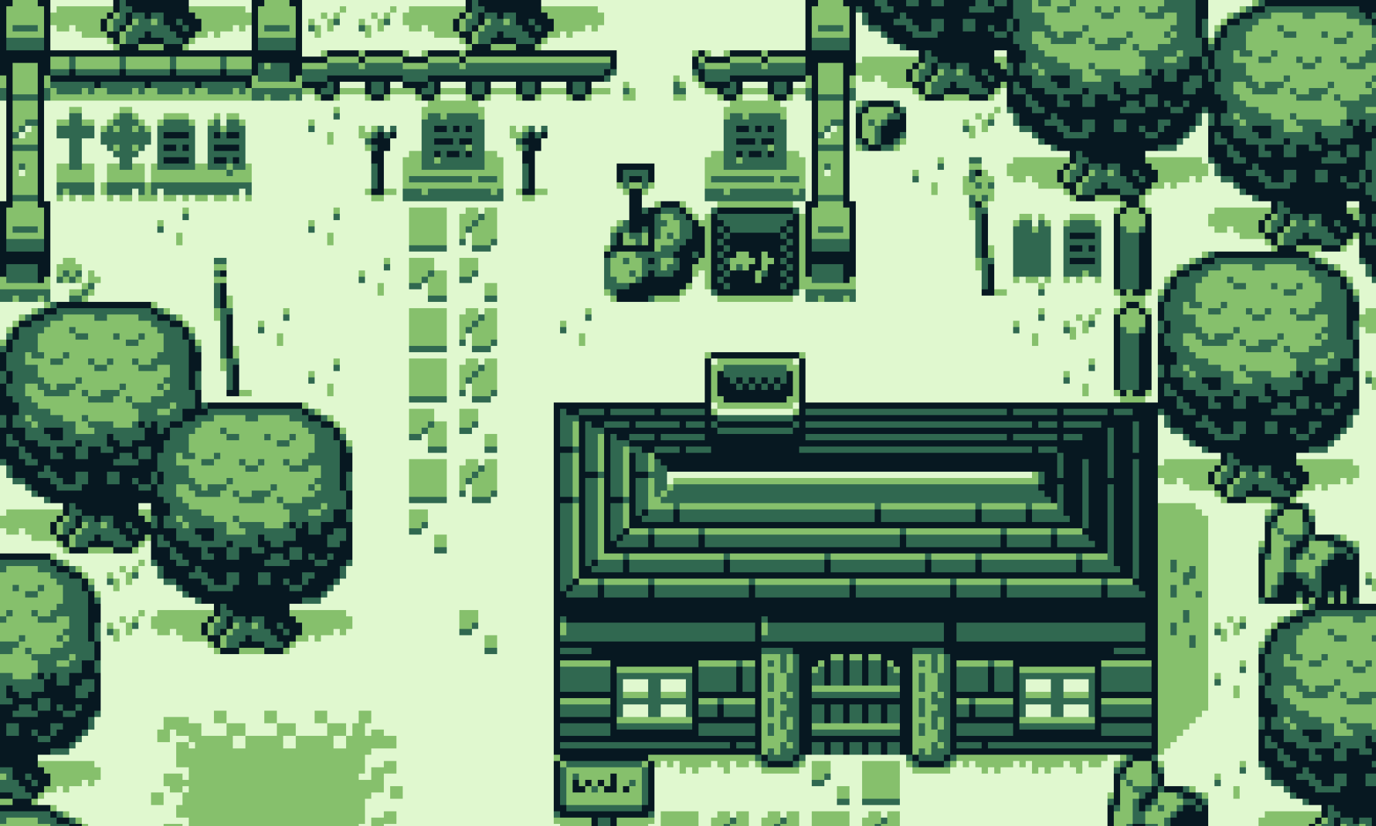
I continued unit testing the PPU and doing complete PPU level single frame and multi-frame tests. I was able to debug a majority of the single frame test cases, but I still have some bugs when rendering frames with more than one sprite. At the moment, I have not integrated the VGA controller logic to test with the FPGA, however, I have been debugging using a custom Python script to render a frame using a pixel array generated using the PPU’s Frame Buffer. Here’s a frame my PPU rendered:

Testing overall has still been a bit of a challenge because in the able of a memory controller and a CPU, my testbench has to be able to simulate the entire environment that the PPU requires. However, I think this is very much worth the effort, as it is likely to make debugging once the full system is integrated much easier. I also spent some time preparing for the Design presentation earlier this week as it was my turn to do the presentation.

Summary of time spent:

  • PPU debugging + adding new tests to the testbench : 8 hr
  • Full-color design updates research: 3 hr
  • Presentation prep + peer review: 3 hr

Schedule / Progress

Overall I think I’m on schedule or slightly behind schedule because I am slightly behind schedule on debugging single frame tests but I started debugging some multi-frame tests and I’ve scoped out what updates/changes will be required for the full-color version. I anticipate that I will be able to get it working full by next weekend.

Next Step

My main goal for next week is to continue debugging the PPU and hopefully also test and profile my implementation a bit after integrating my code with the VGA logic required to test the PPU on the FPGA.
Katherine’s Status Report for 2/22/25

Accomplished:

  • All memory Instructions implemented.
  • Started writing test benches for arithmetic and control flow instructions.
  • Wrote the first draft of CPU parts of the design report.
  • Looked into some other options for the NES USB controller.
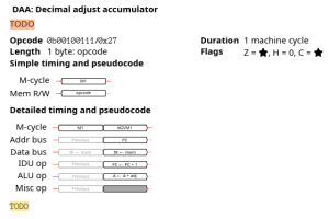
  • Learned what the DAA instruction does (binary coded decimal addition)
Next Step:
  • By the end of spring break, I hope to have a fully implemented CPU that passes all hand-made tests.
Other Notes or Concerns:
  • Progress is ahead of schedule.
  • The Altari controller can be connected directly to GPIO pins. With some modifications it might be a possible substitute for the USB NES controller.

Team Status Report 2/15/25

Progress:

  • CPU:
    • Multicycle CPU framework completed
    • Instructions implemented: 11
    • Instruction tests written: 23
  • PPU
    • RTL updated based on Memory organization / controller related design updates.
    • Implemented testbench, Python script to render image based on frame dump.
    • Unit tested most of the design and parts of the integrated logic. Working on debugging the PPU with a full end-to-end test.
  • MMU
    • Re-designed memory controller to utilize FPGA Block RAMs instead of DE II SRAM/SDRAMs for simplicity of integration
    • Synthesized and tested Block Rams of different sizes (in ROM and RAM variant) and confirmed that they work
    • Creating Memory Controller according to updated spec (DMA support)
  • Other I/O
    • Did research into USB/Audio integration. Discovered that NIOS II cannot be used,  but there are IPs provided by Altera that use an Avalon master/slave interface.
    • Learned more about the Quartus Avalon Slave Interface, currently working to create unit tests
Design Changes:
  • Swapped to cycle-accurate multicycle CPU.
  • Reworked DMA responsibility

Risks and Risk Management:

  • Many CPU instructions are listed as TODO in “Gameboy: Complete Technical Reference”
    • Will look at Intel 8080 and software emulators to fill in the blanks.

Part A – Katherine (public health, safety or welfare):

Our Gameboy will be made as a larger system, similar to a desktop computer, with a larger screen and controller. This will help reduce eye strain, making it easier for users to play games, especially for those with visual impairments. The larger controller will also improve accessibility for people with limited mobility. These modifications will make gameplay less physically taxing, hence improving overall safety.

Part B – Ruslana (social factors):

Our capstone responds to social factors because we intend to make playing the Gameboy an all-inclusive experience at demo day, where anybody can go and engage with the video games. Furthermore, we are preserving the Gameboy’s heritage and legacy by showing others the original and first console ever made that has paved the way for modern ubiquitous consoles all around us today (such as the Switch, Playstation, Xbox, etc.). People who have experienced the original Gameboy and curious younger generations can be both entertained and learn about our hardware implementation for this project.

Part C – Bharathi (economic factors):

Our project offers a cost-effective and sustainable way to preserve and play retro games without relying on original hardware which can be difficult to find, maintain, or upgrade. Unlike a single-purpose handheld console, our FPGA-based design can be upgraded and modified over time without additional hardware costs. Our project also encourages the digital distribution and consumption of retro games through legally obtained ROMs, reducing need for physical cartridges that may become may be hard to find / use.

Katherine’s Status Report for 2/15/25

Accomplished:

  • New CPU multicycle framework completed.
  • Half of the memory instructions pass tests
  • All memory instruction tests were created.
  • Adjusted schedule to account for CPU reworking.
Next Step:
  • Continue implementing memory instructions
  • Start creating control flow instruction tests
Other Notes or Concerns:
  • Progress is well ahead of schedule according to the new schedule.
    • More work has been allocated to spring break to account for CPU reworking.
  • The CPU had to be reworked to be cycle-accurate.
    • Gameboy programmers use the cycles/instruction to create wait loops.
  • The original Gameboy seems to have assumed combinational memory, but our memory is synchronous.
    • Modifications must be done to many of the multicycle instructions that involve memory.
  • Many instructions (20+) are listed as TODO in “Gameboy: Complete Technical Reference”
    • Software emulators and Intel 8080 instructions will be used to figure out what these instructions do.

Ruslana’s Status Report for 2/15/25

  • Re-evaluated memory spec with Katherine and Bharathi
  • Held a design review with Bharathi on her PPU implementation
  • Re-worked DMA specification with Katherine and Bharathi and memory size of each Block RAM
  • Learned more about Avalon slave interface to communicate with peripherals (SRAM, audio)
  • Writing Memory Controller (with updated DMA, newly Quartus generated Block RAMs)
  • Writing unit tests for USB/Audio –> will test by Sunday

Bharathi’s Status Report for 2/15/25

Accomplished

My goal for this week was to update the RTL for the PPU to work in accordance with the Memory Controller and testing my implementation so far.

I have unit tested a majority of the phases and more complex sections of my design like the object sorting, scrolling + window + background overlay logic, and switching between different modes, scanlines, and frames. I updated my testbench to include an end-to-end test for the PPU where I simulate the VRAM, OAM, control register reads and writes but I have not completed debugging the full design. At the moment, I have not gotten my hands on a DE2-115 FPGA so I haven’t been able to test the VGA controller logic on an FPGA, however, I wrote a Python script that uses a frame dump (2D pixel array) as an input and generates an image for debugging purposes.

I finished up the slides for the design presentation and updated it based on the feedback we got during our weekly meeting. I also spent some time preparing for the presentation next week.

Summary of time spent:

  • PPU design updates based on Memory Controller: 2 hr
  • Scoping cases to test + implementing testbench: 4 hr
  • Integrating design part-by-part + debugging: 6 hr
  • Presentation Slides + prep: 3 hr

Schedule / Progress

I am slightly ahead of schedule overall having already debugged majority of the individual components of the design. Integrating the phases, multiple state machines, and timing logic part by part lead me to spend more time writing the testbench than working on the design but I believe it sped up the debugging process overall quite a bit.

Next Step

My main goal for next week is to debug the PPU end-to-end and make any updates required for integration with the Memory Controller. I intend to hopefully test my PPU on the FPGA with the VGA Controller and be able to fully render a frame by end of next week.

Team Status Report 2/8/25

Progress:

  • CPU:
    • All frameworks completed.
    • Instruction buffer added.
    • Instructions implemented: 2
  • PPU
    • RTL completed based on datapath.
    • Testbench development in progress.
  • MMU
    • Re-designed memory controller to utilize FPGA Block RAMs instead of DE II SRAM/SDRAMs for simplicity of integration
    • Synthesized and tested Block Rams of different sizes (in ROM and RAM variant) and confirmed that they work
  • Other I/O
    • Did research into USB/Audio integration. Discovered that NIOS II cannot be used,  but there are IPs provided by Altera that use an Avalon master/slave interface.
Design Changes:
  • Swap to 32-bit word memory is under consideration.
  • Swapped memory units for BRAM

Risks and Risk Management:

  • If a swap to 32-bit words is confirmed, a full reworking of the instruction buffer will be required.
    • CPU will be developed with the assumption of 16-bit words until told otherwise since the 16-bit word architecture is harder to implement.
    • To make the possible transition easier, we will mark all code that must be removed or replaced if this change occurs.
  • Memory has been tested but I/O parts still need to be confirmed ASAP.

Ruslana’s Status Report for 2/8/25

  • Researched memory options on FPGA DE 2 board (block rams, SDRAM, SRAM, Flash) and explored options through Quartus Megawizard IP Interface
  • Discussed with Professor Nace for potential options on FPGA memory
  • Derived new design based on FPGA Block RAMs based on discussion with Bharathi and Katherine on CPU/PPU accesses
  • Re-designed Memory Controller Datapath to utilize block RAMS
  • Obtained DE II 115 boards from Quinn and distributed it to members
  • Created 5 generic memory modules for Block RAM
  • Created testbench for each memory module in simulation and Chip Interface
  • Synthesized and tested BROMs/BRAMs on FPGA and confirmed success by empirical validation
  • Did research into audio/USB integration and realized NIOS II is a soft-core processor that you can write C code for, but it gets synthesized onto the FPGA and uses up the LUTS. It’s a way to give people an easy route to write C code to be used on FPGA, but not on on-chip computer that talks to the FPGA itself.
    • FPGA University Program on Quartus ECE Machines gives some kind of Qsys interface to create USB and Audio IP devices? Requires further research.

Bharathi’s Status Report for 2/8/25

Accomplished

My goal for this week was to finish my datapath for the PPU and get the RTL complete so I can begin testing next week.

I have completed the RTL and verified that my code is synthesizable. I tested some of the smaller modules dedicated to sprite searching and pixel/frame buffering. I have already started working on the testbench which is my main task for next week. I also helped Ruslana with research into some FPGA memory use questions.

I also spent some time this week working on the slides for the design presentation and did some research into effectively mapping out some of our qualitative use-case requirements to more testable quantitative design requirements.

Schedule / Progress

As I have already started working on the testbench and I am also almost done with my design presentation slides, I think that should put me well ahead of schedule at the moment.

Next Step

My main goal for next week is to debug as many single-frame rendering cases as time allows. I’ve mapped out about 20 different edge cases across sprite priority, sprite search, FIFO and memory related operations that need to be tested.  I expect this round of testing to be somewhat involved because my testbench needs to be able to simulate everything — memory, CPU updates to control registers, interrupt handling etc.

I also plan to finish up any updates to my design presentation slides based on feedback and start preparing for the actual presentation.

Katherine’s Status Report for 2/8/25

Accomplished:

  • Proposal presentation thouroghly practiced and given.
  • CPU testbench framework made for ModelSim.
    • Tests can be easily added to the testbench.
    • Can pick which test to run from the terminal.
  • CPU basic framework completed.
    • ld r,n (load immediate) passes handmade tests.
    • ld r,r’ (move) passes handmade tests.
  • Instruction buffer implemented and passes handmade tests.
Next Step:
  • Implement all memory instructions.
  • Make handmade tests for all memory instructions.
Other Notes or Concerns:
  • Progress is slightly ahead of schedule.
  • Memory and control flow operations are being prioritized so the other units can be tested using ROMs