My goal(s) for this week were some subset of:
- Get DMG PPU integrated with CPU (if CPU gets integrated with memory)
- Fix scrolling / sprite bug in DMG PPU
- Debug CGB PPU
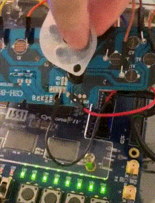
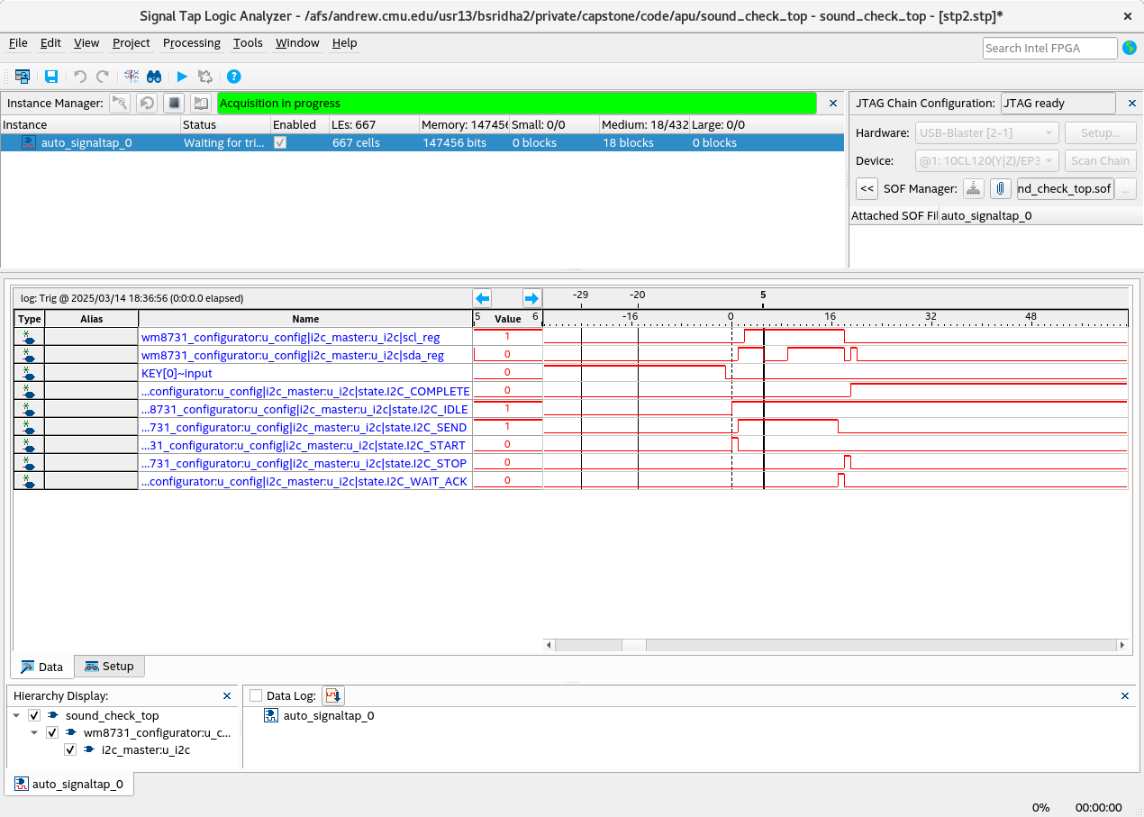
- Attempt to read from and write to WM8731 using i2c and get some confirmation that it was configured correctly.
Accomplished
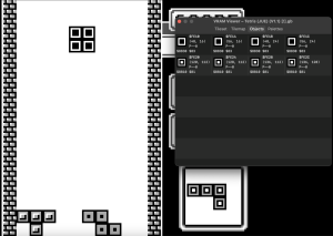
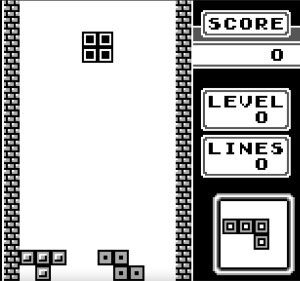
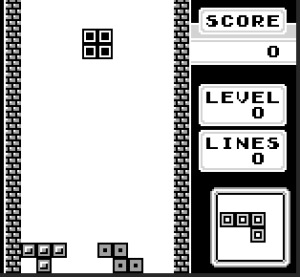
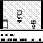
DMG PPU (4-color PPU)
I fixed a few more bugs, and wrote a new testbench to do the equivalent of the dmg-acid2 test. Ruslana and I also performed a basic VGA test which was successful, and I have integrated the updated VGA logic with my PPU.
CGB PPU (full-color PPU)
I propagated bug fixes from the DMG version to the CGB version. The CGB PPU now renders basic backgrounds with hardcoded color palettes.
APU / CODEC Research
I also implemented a basic test on the WM8731 by writing to the reset register. This test appears to be successful so I have implemented the full WM8731 configuration i2c logic to set 10+ registers and setup i2s communication.

Summary of time spent this week
- VGA test: 2 hrs
- WM8731 Reset test: 5 hrs
- WM8731 Full Configuration implementation + simulation debug: 8 hrs
- DMG debugging + CGB updates: 3 hrs
Schedule / Progress
Overall, I’m very much on schedule. I don’t have any concerns regarding getting the full PPU working once we get everything integrated (as the PPU is fairly well tested in my opinion). The APU still remains a bit of a risk, however, using the CODEC directly now definitely seems viable.
Next Step(s)
- Validate full WM8731 configuration.
- Sketch I2S implementation (+ test with basic wave on FPGA).
- DMG PPU integration.
- CGB PPU debugging — target: get backgrounds and windows working.