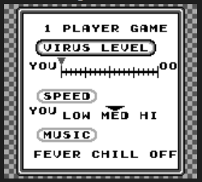
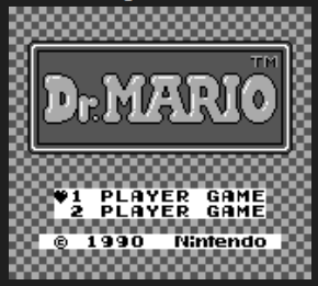
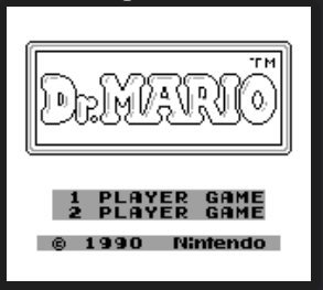
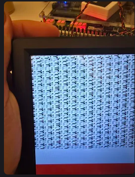
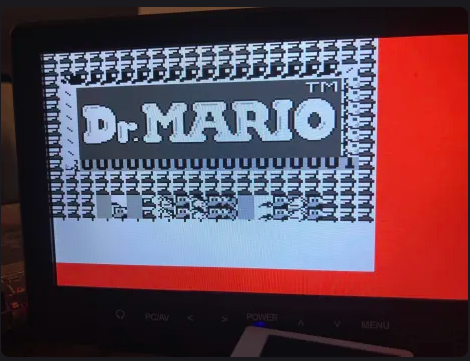
Debugged Tetris and Dr.Mario on VGA with team. Tetris looks mostly functional but the game appears to run 2x faster. Dr.Mario is stuck after the pill is spawned & before it is thrown.
I spend some time debugging the issue on simulation. Sadly, this was a fairly slow process as many of the bugs in the games we want to play show up somewhat later so I need to run the simulation for a while to get more information but this still offers a lot more visibility so I am optimistic that I will be able to debug the issue with Dr Mario and Tetris.
Katherine and I also plan to test a few other games on synthesis.
Debugged DMG Acid Test — frame rendered appears to be fully correct. Also fixed the missing hand issue on Dr.Mario in simulation.
Debugged Tetris and Dr.Mario on VGA with team. Tetris looks mostly functional but the game appears to run 2x faster. Dr.Mario is stuck after the pill is spawned & before it is thrown.
Fixed synthesis issues related to the Audio Test. Technically we have all the pieces for the APU but integrating it is likely to introduce a number of other issues so I have postponed it until we get Dr.Mario and Tetris working perfectly.
Ruslana and I spent a lot of time investigating the Dr Mario pill issue on simulation. Unfortunately, the bug happens after such a long time that looking at in simulation is not the most productive way to attacking the problem. However, simulation allowed us to get more specific areas / registers / addresses to look at.
Schedule / Progress
We are somewhat behind schedule given the APU status but otherwise integration is going pretty well.
Next Step(s)
Finish debugging Dr.Mario and Tetris.
Potentially integrate APU.
Tools/knowledge:
We need to learn the GameBoy spec thoroughly to implement it correctly. The largest challenge with this was trying to parse the many informal / unofficial documentation (that was usually contradictory).
I also learnt a lot related to Intel / Altera tooling and designing specifically for FPGAs. Prior to this, most of my hardware experience had been on simulation.
Implementing the PPU from scratch also forced me to explore more new and complex strategies to testbench my code (both separately and after integration).
I also got plenty of practice using wave viewers and software debuggers during debugging.
We are able to render specific frames statically with Tetris/Dr.Mario/other rom tests in simulation now, but rendering the full game code in synthesis is still being debugged.
Successfully generated first frame for Tetris in simulation.
Successfully generated 3 frames for Dr Mario using actual Joypad interrupts in simulation.
VGA Support added in synthesis.
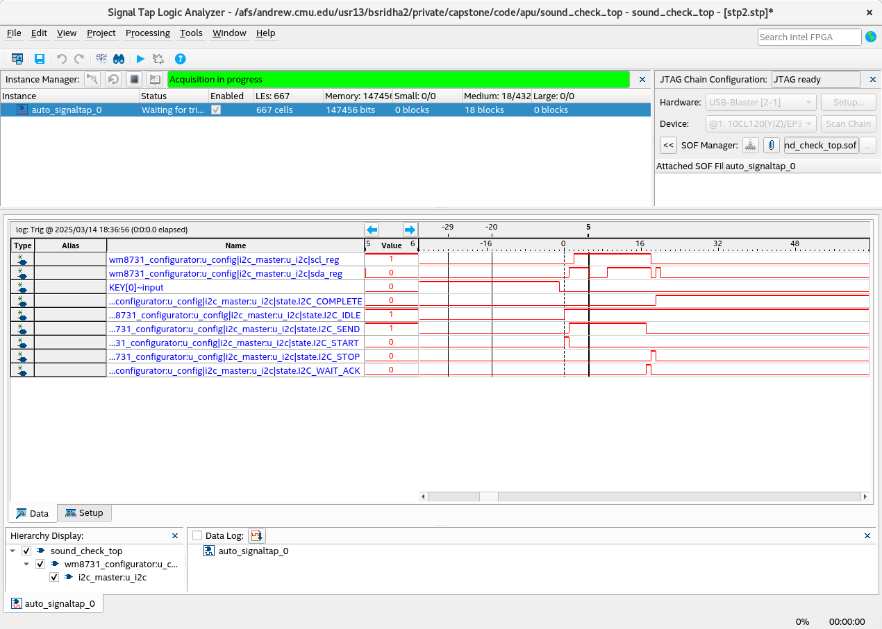
Full design (including controller) integrated and synthesized on FPGA — debugging (using SignalTap 🙁 ) in progress.
DMG Acid Test face runs and shows up as a mostly intact fact on synthesized design
Dr. Mario ROM in synthesis has yet to work–after starting it up on an FPGA, the first frame shows up as a flicker and then it’s a white screen. We are fixing this currently.
PPU: DMG Acid Test in simulation almost fully debugged. PPU integrated with design fully. VGA + BRAM based Frame Buffer support added.
PPU clock that runs at 4MHz (1 cycle is called a dot)
CPU clock that runs at 1MHz (1 M-cycle = 4 dots)
VGA clock that runs at 50MHz
The reason for these clocks is due to the spec.
The MMU must run twice the CPU frequency, because our FPGA BRAMS (gameboy memory) have a 2 cycle read latency.
The PPU is clocked at 4 MHz according to Gameboy spec
The CPU executes an instruction across 4 cycles of the 4 MHz clock–hence, we made the CPU clocked according to 1 MHz. This is a subtle distinction that took us a while to dig out during integration and clarify. The discrepancy between the CPU and PPU clocks are documented poorly online and likely isn’t as big of a concern for software emulators.
The VGA must communicate at 50 MHz.
In our FPGA, we have two clock generators – a 50 MHz one and an 8 MHz one. The other 4 MHz and 1 MHz signals are derived from the 8 MHz to ensure that the clock edges are properly aligned. This was another bug we fixed this week.
Risks and Risk Management:
Switching to Joypad GPIO for now to reduce USB integration complexity
Postponing NIOS II integration for after MVP gets hit, especially because its more well understood now
Potentially cutting APU from final, because of time considerations (even though the pieces to put it together exist)
Verification & Validation Progress:
CPU:
passes Blargg Test ROM cpu-tests (minus interrupt tests due to optimizations in PPU)
passes hand-made tests
Is able to generate multiple frames and process joypad input.
PPU:
Passes mode-level, line-level, and frame level timing requirements
100% palette mapping accuracy
Minor Sprite bugs – but these will be debugged soon to achieve sprite accuracy requirement
Frame Output latency well under requirement threshold
MMU:
Passes in personal testbench that did:
Queries to memory regions (rom/wram/exram/vram/oam/hram)
Queries to memory IO registers
DMA Query
Basic interrupt checks
APU: Work in progress – no tests have been done so far
I/O:
All key presses on the controller are very responsive – complete testing of latency will be done soon to validate if controller response time meets use case and design requirements.
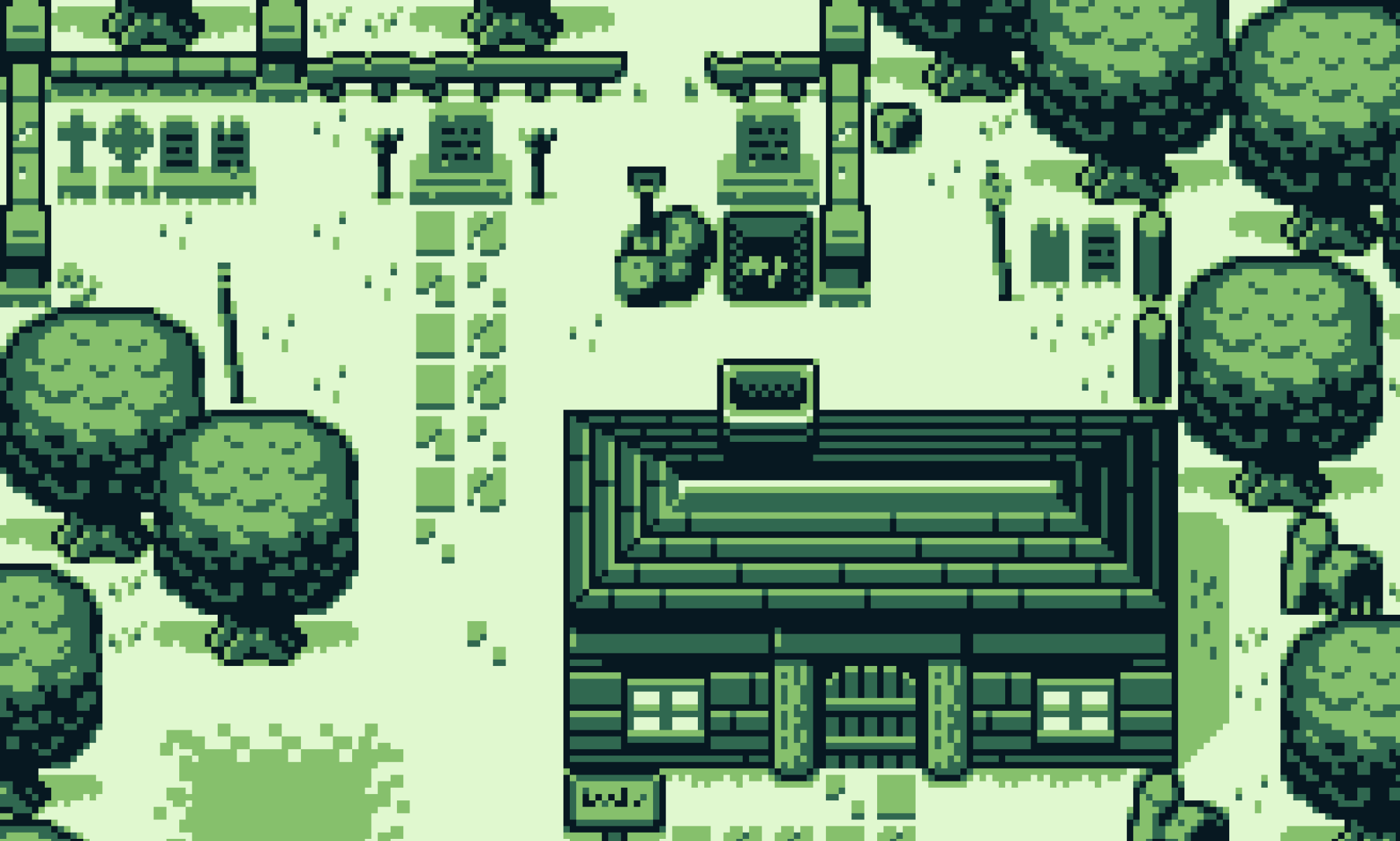
Spent a lot of time debugging the many edge cases part of the DMG Acid Test. DMG PPU pretty close to being done and looks almost perfect:
DMG Acid Test — Fully Integrated VersionDMG Acid Test — Reference Image
CGB PPU (full-color PPU)
No updates here.
APU / CODEC Research
Acquired 3.5mm TRS connector for testing on APU.
Discussed the APU design / implementation with Ruslana.
Researched audio output for APU.
Summary of time spent this week
Integration debugging: 20+ hrs
APU / Audio research: 2+ hrs
DMG Acid Test debugging: 10+ hrs
Schedule / Progress
I believe I’m on schedule and integration going well. We spent a lot of time debugging on simulation and we’ve made great progress fixing a number of different bugs across our design. Our next goal as a group would be get something that is moderately playable by next week.
Next Step(s)
More integration debugging (this time on FPGA).
Final presentation stuff.
APU test on FPGA.
Verification & Validation information is part of our Team Status Report.
DMG PPU integration (in progress, to be continued).
APU test on FPGA (postponed to next week).
Accomplished
DMG PPU (4-color PPU)
PPU integration is in progress.
Integration & debugging in progressAfter fixing Scrolling (SCX, SCY) and LCDC related bugsDMG Acid Test — Reference Image
CGB PPU (full-color PPU)
No updates here.
APU / CODEC Research
Postponed work on APU in favor of getting the PPU integrated and preparing for the demo.
Summary of time spent this week
PPU & integration debugging: 12+ hrs
Schedule / Progress
I believe I’m on schedule. Integration is in progress. PPU and MMU are fully integrated, and our test to render a single frame was successful. CPU, MMU, PPU all seem to be talking well but there’s still a lot of integration debugging left.
Validate full WM8731 configuration (postponed to next week).
Sketch I2S implementation (completed).
DMG PPU integration (postponed to next week).
CGB PPU debugging — target: get backgrounds and windows working (completed).
Accomplished
DMG PPU (4-color PPU)
No updates here, I plan to integrate this with the CPU & MMU early next week.
CGB PPU (full-color PPU)
Backgrounds seem to be mostly functional, but I’m still debugging issues with the sprite palettes.
APU / CODEC Research
Implemented I2S logic — works in simulation.
Sketched datapath for APU + wrote some RTL. Will do a code review for this with Ruslana next week and try a basic test on FPGA.
Summary of time spent this week
CGB debugging: 9+ hrs
I2S implementation: 2 hrs
APU research + datapath + RTL: 4 hrs
Schedule / Progress
I believe I’m on schedule. I don’t have any new concerns about the PPU or APU largely, but I should really integrate the PPU next week so I can debug some larger tests.
Get DMG PPU integrated with CPU (if CPU gets integrated with memory)
Fix scrolling / sprite bug in DMG PPU
Debug CGB PPU
Attempt to read from and write to WM8731 using i2c and get some confirmation that it was configured correctly.
Accomplished
DMG PPU (4-color PPU)
I fixed a few more bugs, and wrote a new testbench to do the equivalent of the dmg-acid2 test. Ruslana and I also performed a basic VGA test which was successful, and I have integrated the updated VGA logic with my PPU.
CGB PPU (full-color PPU)
I propagated bug fixes from the DMG version to the CGB version. The CGB PPU now renders basic backgrounds with hardcoded color palettes.
APU / CODEC Research
I also implemented a basic test on the WM8731 by writing to the reset register. This test appears to be successful so I have implemented the full WM8731 configuration i2c logic to set 10+ registers and setup i2s communication.
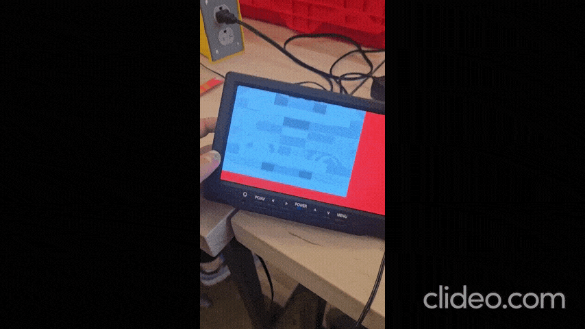
SignalTap screenshot of reset test on FPGA using WM8731Full Configuration works in Simulation
Summary of time spent this week
VGA test: 2 hrs
WM8731 Reset test: 5 hrs
WM8731 Full Configuration implementation + simulation debug: 8 hrs
DMG debugging + CGB updates: 3 hrs
Schedule / Progress
Overall, I’m very much on schedule. I don’t have any concerns regarding getting the full PPU working once we get everything integrated (as the PPU is fairly well tested in my opinion). The APU still remains a bit of a risk, however, using the CODEC directly now definitely seems viable.
Next Step(s)
Validate full WM8731 configuration.
Sketch I2S implementation (+ test with basic wave on FPGA).
DMG PPU integration.
CGB PPU debugging — target: get backgrounds and windows working.
Full-color (CGB) implementation done, debugging in progress
MMU
MMU has been written, undergoing debugging and soon-to-be integrated
APU
APU writing has started and will be completed soon. Debugging postponed until after MMU/PPU/CPU integration.
Research into how to use WM8731 (Audio CODEC on the DE2-115)
Implemented simple I2C based sound check test for the WM8731
Other I/O
Spent a lot of time researching USB integration
Confirmed GPIO NES controller works.
Resolved NIOS II blocker of lacking library support (had to source specific directory and add to LD_LIBRARY_PATH)
Design Changes:
Block RAMS are all 16 bit-width, 2 column format (given that the original gameboy’s data is 8 bit data words).
The reason for this is because we can instantiate dual port RAMS with 16 bit width that can allow OAM entries (32 bit wide) to be accessed in a single clock cycle by the PPU
Leaving other Block RAMS as 16 bit width as well is reasonable for the CPU and makes things consistent
Risks and Risk Management:
Switching to Joypad GPIO for now to reduce USB integration complexity
Postponing NIOS II integration for after MVP gets hit, especially because its more well understood now
Additional Information:
A was written by Bharathi, B was written by Katherine and C was written by Ruslana
Part A — Global factors:
Emulators such as our project help preserve classic video games by allowing people to play them on modern devices, even after the original hardware becomes obsolete. This has global importance, as it makes retro games accessible to people everywhere, regardless of location or resources. Additionally, studying older gaming systems through emulation helps developers understand how past technologies shaped current gaming, inspiring innovation for the future. Our project not only keeps the GameBoy experience alive but also contributes to preserving gaming history on a global scale.
Part B — Cultural factors:
The Gameboy, The console that popularized handheld gaming devices, was discontinued in 2003. It was a significant milestone in gaming history, being the start of many beloved franchises such as Pokemon. However, as time passes, these games, especially lesser-known titles such as Dr. Mario, are fading into obscurity. Our Gameboy emulator helps preserve this gaming history and provides a pathway for the gaming community to reconnect with its roots.
Part C — Environmental factors:
There are several environmental considerations on how our choice to emulate a Gameboy using an FPGA. The greatest benefit of our choice to use an FPGA is the inherent reconfigurable capabilities of an FPGA compared to an ASIC. FPGA development boards can be reprogrammed to serve completely different purposes, and do not require manufacture of new chips. In fact, we were able to avoid incurring any actual cost in our project because FPGAs already exist in the inventory. Once we complete our project, the FPGA can simply be returned and reused for a completely different purpose–therefore, we generate no E-waste with our project.
In addition, if our project succeeds and we open source our FPGA capstone project to other people, they also may be encouraged to enhance or build upon our work. This also can reduce material consumption in the greater community.
My goal for this week (and break) was to mainly finish debug the PPU and get started on the full color implementation.
DMG PPU (4-color PPU)
I spent most of my time this week on getting the DMG PPU fully functional—and I was pretty successful! I decided to rewrite the testbench so that it would also generate the final image (in PPM format) so I wouldn’t need to use a Python script. This sped-up my debugging progress considerably.
The other main breakthrough with debugging came in the form of SameBoy (GameBoy emulator), which I used to get the VRAM data and the OAM data for each frame. This method is not perfect as it doesn’t really give me information for crucial control registers that can change on a line by line basis. However, it helped me find many of the weirder bugs in my PPU a lot more quickly.
SameBoy Emulator
The DMG PPU is very close to being done. I still have minor issues with certain sprite and scrolling edge cases, however these frames (or sequence of frames) involve CPU writes to VRAM so I have no way of verifying if the issue is with my RTL or simply because I don’t have the perfect snapshot of the memory.
In summary, I’m pretty happy with the progress and feel confident moving onto working on the full-color PPU. Here are some frames I rendered this week:
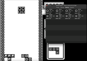
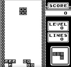
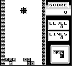
Tetris — Reference (from SameBoy)
Tetris — Frame I rendered
CGB PPU (full-color PPU)
I used the information I collected during the prior week to make the necessary updates for the full-color PPU. Because of my modular design of the rendering pipeline, I am able to make changes on the DMG PPU but still treat the layers as “black boxes” in some sense and extrapolate to make the CGB PPU integrated with larger memory sizes, many more color palettes and many new edge cases.
APU / CODEC Research
Given the NIOS / Quartus based roadblock we hit last week, I spent some time researching alternative solutions with Ruslana. The most promising approach is directly using the CODEC (WM8731) without using the NIOS softcore by configuring the registers on the WM8731 using i2c and then transferring the actual data using i2s. This appeared to be quite complex at first, especially because we weren’t able to find any evidence that someone else had managed to do this. But we’ve recently found some labs (form digital design classes at other universities who also using the same FPGA) that implement different fragments of the logic on the WM8731 directly.
I plan to use very simple i2c based test with the WM8731 to see if we get an ACK after a write to the reset register on WM8731. This should help us evaluate on the feasibility of using this approach for the APU.
Design Report
I also spent a decent chunk of time working on the design report the week it was due. We ended up working almost until the deadline as we received some crucial feedback from our design presentation somewhat late, but we were able to make the necessary updates before the deadline.
Summary of time spent (Week of 2/23 to 3/1):
Researching how to use WM8731 (Audio CODEC on the DE2-115): 6 hrs
Design Review Report: 8 hrs
Summary of time spent (Week of 3/2 to 3/8):
Writing new testbench: 2 hrs
PPU debugging + VGA testing : 12 hrs
Full-color (CGB) implementation: 3 hrs
Writing I2C based sound check test for the WM8731: 2 hrs
Schedule / Progress
Overall I’m on schedule or maybe slightly ahead as I feel relatively confident about the correctness of the DMG PPU (wrt to our MVP games — Tetris and Dr Mario should both be pretty much correct as they have no scrolling). I will also likely be spending some sizable amount of time on the APU from this week onwards as that remains as our largest unknown at the moment.
Next Step(s)
My goal(s) for next week are some subset of:
Get DMG PPU integrated with CPU (if CPU gets integrated with memory)
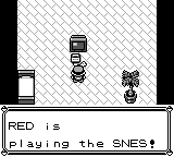
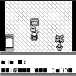
Fix scrolling / sprite bug in Pokemon Red:
Correct Frame (from SameBoy)Frame I rendered
Debug CGB PPU
Attempt to read from and write to WM8731 using i2c and get some confirmation that it was configured correctly.
My goal for this week was to debug the PPU and scope out what updates would be necessary for the full color implementation.
I continued unit testing the PPU and doing complete PPU level single frame and multi-frame tests. I was able to debug a majority of the single frame test cases, but I still have some bugs when rendering frames with more than one sprite. At the moment, I have not integrated the VGA controller logic to test with the FPGA, however, I have been debugging using a custom Python script to render a frame using a pixel array generated using the PPU’s Frame Buffer. Here’s a frame my PPU rendered:
Testing overall has still been a bit of a challenge because in the able of a memory controller and a CPU, my testbench has to be able to simulate the entire environment that the PPU requires. However, I think this is very much worth the effort, as it is likely to make debugging once the full system is integrated much easier. I also spent some time preparing for the Design presentation earlier this week as it was my turn to do the presentation.
Summary of time spent:
PPU debugging + adding new tests to the testbench : 8 hr
Full-color design updates research: 3 hr
Presentation prep + peer review: 3 hr
Schedule / Progress
Overall I think I’m on schedule or slightly behind schedule because I am slightly behind schedule on debugging single frame tests but I started debugging some multi-frame tests and I’ve scoped out what updates/changes will be required for the full-color version. I anticipate that I will be able to get it working full by next weekend.
Next Step
My main goal for next week is to continue debugging the PPU and hopefully also test and profile my implementation a bit after integrating my code with the VGA logic required to test the PPU on the FPGA.