
Accomplished
My goal for this week was to update the RTL for the PPU to work in accordance with the Memory Controller and testing my implementation so far.
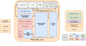
I have unit tested a majority of the phases and more complex sections of my design like the object sorting, scrolling + window + background overlay logic, and switching between different modes, scanlines, and frames. I updated my testbench to include an end-to-end test for the PPU where I simulate the VRAM, OAM, control register reads and writes but I have not completed debugging the full design. At the moment, I have not gotten my hands on a DE2-115 FPGA so I haven’t been able to test the VGA controller logic on an FPGA, however, I wrote a Python script that uses a frame dump (2D pixel array) as an input and generates an image for debugging purposes.
I finished up the slides for the design presentation and updated it based on the feedback we got during our weekly meeting. I also spent some time preparing for the presentation next week.
Summary of time spent:
- PPU design updates based on Memory Controller: 2 hr
- Scoping cases to test + implementing testbench: 4 hr
- Integrating design part-by-part + debugging: 6 hr
- Presentation Slides + prep: 3 hr
Schedule / Progress
I am slightly ahead of schedule overall having already debugged majority of the individual components of the design. Integrating the phases, multiple state machines, and timing logic part by part lead me to spend more time writing the testbench than working on the design but I believe it sped up the debugging process overall quite a bit.
Next Step
My main goal for next week is to debug the PPU end-to-end and make any updates required for integration with the Memory Controller. I intend to hopefully test my PPU on the FPGA with the VGA Controller and be able to fully render a frame by end of next week.