Nancy’s Status Report for 4/12

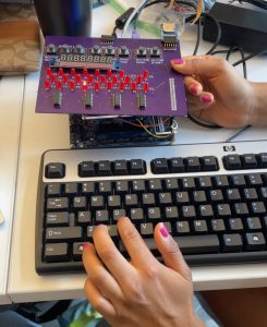
The past two weeks, Amelia and I have made good progress on the RTL. We currently have a working implementation of the rotary encoder, which can change the number displayed on the on-board 7 segment displays, but we do have some strange jumping issues when we try to implement it by scrolling through the alphabet, since there is some unexpected behavior on reset.  Additionally, we spent the majority of our time working on the external seven segment display that uses the MAX7219 chip. We had a lot of trial and error trying to adapt Arduino library code and existing RTL code (that was in VHDL, not Verilog) to work in Verilog. We used an Arduino to verify that the display itself worked, but after a lot of debugging, we successfully displayed a message early this week!

Later this week, Amelia and I worked on expanding our implementation of the variable rotor settings. For our demo, we only had users change the rotor starting setting (A-Z), but still hardcoded the rotor type (1-5) and ring starting setting (A-Z). On Friday, we spent most of the day implementing this and got all of the settings to display on the external 7 segment display! These settings could all be changed using the switches and buttons on the DE-10 and we verified that changing these settings reflected in accurate encryptions using an online Enigma simulator.

Now that the PCB has arrived, Amelia and I need to start wrapping up our RTL. This week, we will work on the shift registers for the lampboard, which should be pretty simple, and we will debug the rotary encoder implementation too. This will keep us on schedule.

As Amelia and I have been working on the RTL, it was very helpful to verify the individual components along the way. This made integrating them much easier. For example, we first got the rotor settings to display on the on-board DE-10. Using the on-board I/O (buttons and switches), we verified that the rotor settings could be changed and that they were correct when compared to the original Enigma machine using an online simulator. This included focusing on edge cases like the wrap-arounds from Z-A and the transitions at the knockpoints, which cause the other rotors to rotate as well. We also individually tested that the 7 segment display worked, and then incorporated that with displaying the actual settings. We will continue to run these targeted tests around edge cases and plan on conducting user testing to see how people who are not familiar with the design will interact with it. We want to ensure that the encryption is always 100% correct.


Nancy’s Status Report for 3/29

In the beginning of the week, Tanisha and I worked on routing the PCB, especially figuring out the routing around the shift registers and how best to organize the many LEDs/resistors to minimize trace complexity. Once she had finished the rest of the routing, we also worked to fix an issue with the 3.3V/GND pours on Fusion and I reviewed the layout one more time before Tanisha placed the order.

In the later half of the week, Amelia & I spent a lot of time in 1305 debugging the integration of the encryption modules with some basic GPIO using the buttons, switches, and 7-segment displays that already exist on the DE-10. This is a good stepping stone towards incorporating the GPIO from our PCB and also gives us a good way of demonstrating our progress in our interim demo.

More specifically, we initially had issues with the encryption itself being incorrect. One issue is that our 3rd rotor needed to be “rotated” once before encryption, so it was as if the first rotor started on Z when we expected it to be on A. While this was a quick fix, we also realized that we were overlooking the break code component of the PS/2 protocol. By incorporating an FSM that could alert our other modules of when a key was released (and therefore the break code was sent), we were able to fix our encryption and have the cryptographically correct result display when (and only when) the key was being held down on our external keyboard. This mimics how the lampboard will light up only when a key is pressed. Next, we moved onto incorporating more I/O. For the demonstration, we decided to make the starting rotor position for all 3 rotors variable, where switches would select which rotor to rotate and a button would allow you to cycle through the alphabet. After a day spent debugging this implementation, we successfully translated “Hello” to ciphertext and back on Saturday night! Here is a video of it working.

Next week, Amelia and I plan to work on capstone in the first half of the week before Carnival. We aim to incorporate the rotary encoder FSM that I wrote with our existing design and start on the I2C communication for the MAX 7-segment display. This will keep us on schedule since we want to have as little difficulties as possible incorporating the PCB by making sure the individual I/O components can work with our Verilog.

Team Status Report for 3/29

This week the PCB team finished working on the PCB and sent it to order. The challenges we faced were dealing with Fusion 360 irregularities, double checking all our safety checks, and figuring out our ordering strategy. Since it would take a longer time than we anticipated we had to select the rush order option which ate up a portion of our safety chunk of our budget. However, since we have spent a longer time on the PCB than we anticipated, we are also more confident in its ability to work correctly and are still well within budget. A challenge we foresee would be on board PCB debugging but since we have mitigated everything we could on the pre-manufacturing end I am confident in our abilities to make this succeed. More challenges we had to deal with was just planning out spacing on the board to maximize aesthetics, cost, functionality and speed of delivery.

The Verilog team has been working consistently this whole week to integrate the encryptions with the interfacing of the PS/2 keyboard. They have successfully managed to get a user input from the keyboard, encrypt it and display this to the onboard 7-segment display on the FPGA!! This came with more than it’s fair share of challenges however – handling flashing break codes between encryptions, random letters being encrypted upon first key press, and debouncing algorithm complexity. This is all being done in preparation for our Interim Demo this upcoming week.

As a team we plan to present this working encryption input and output scheme alongside our PCB narrative and final design. We will discuss our use case briefly before moving on to talk about the challenges each of us faced throughout this process – something that has also been detailed through all our status reports. This would be the majority of our work for the upcoming week.

Our team also met with Professor Chang this week to discuss our design layout plans. Since we last spoke to her we had switched to an external keyboard as she recommended for user friendliness, however as we are now doing a PS/2 keyboard we were limited by the vintage offerings (and power considerations – see team status report 3/15). She approved of our PCB layout and user interface and advised us on possible enclosure ideas. We decided that could be a stretch goal for us after completing all of the functionality.


Tanisha’s Status Report for 29/3

This week I finished all of the routing of the PCB and ordered it [final version attached]. After routing I went through our completion checklist (pours, rechecked documentation for all pinouts, ran ERC and DRC, ensured trace width safety of 10 mils, and all relevant silkscreening was included). There were a few challenges with Fusion 360 during this checklist but I managed to resolve all issues (e.g. errant wire stubs that simply would not disappear, heavily cleaned up routing, and re-organization of components and pins). When it came to ordering we faced another challenge with realizing manufacturing time was not built into the previous OshPark measurements we had looked into previously. This led to us weighing the costs of different sped up manufactoring options vs possibly pivoting back to JLCPCB from China but facing the risk of getting our PCB stuck at customs similar to other PCB orders from CMU. However, after a team discussion I went forward with the expedited order option and hope to have it arrive and start soldering immediately after Carnival.

The rest of our ordered parts also arrived, the new SD Card Reader, SD Cards and SMD resistors.

I also prepared for our Interim Demo by creating slides for our use case and my progress. I plan to distribute print outs of our PCB design iteration process and talk through the challenges faced and the different changes between each of them. I think this well encapsulates the work I’ve put in for this project over the past few months. I also plan to lay each of the individual parts out (rotary encoder, MAX7219, SD card reader, LEDs, resistors etc) so that our showcase would display a clear idea of what our PCB consisted of.

This week I plan to work on our Interim Demo and help with overall Capstone tasks. That would include start thinking about our Final Presentation, individually test our GPIO and figure out the new SD cards and reader integration.


Team Status Report for 3/22

This week, we have made good progress on both the embedded and Verilog side. One significant risk is that our peripheral components will not be compatible with the FPGA, which will be difficult to fix once they are solidified on the PCB. We are managing this by testing and researching these components beforehand, such as the microSD card reader. This way, we can change or find new components before we get the PCB fabricated. This has led to a possible change, since we have ordered two different microSD card readers out of concern that the original one won’t be compatible with the FPGA’s 3.3V logic. Once the microSD cards come in, we can verify if we can move forward with this option. Other than that, no changes to the existing design have been made this week.

Another risk is that the individual RTL components will not integrate properly. We are mitigating this by testing the integration of individual modules after they are individually validated. This is the current phase we are in for the RTL, since Amelia has validated that the PS/2 works in simulation and synthesis, the encryption in simulation, and the PS/2 and encryption together in simulation. However, we have not yet succeeded in integration the PS/2 and encryption in synthesis, and is what we will be working towards this week.

Nancy’s Status Report for 3/22

This past week, I worked on the microSD card implementation. I tried to test our microSD card reader with a multimeter to see what its idle voltage was (3.3V or 5V) but after doing some more research, I realized that the microSD card must be inserted in order to activate pull up resistors in the reader. So, while we waited for the microSD card to arrive, I started on the RTL of the microSD card reader, which is SPI protocol. I found a resource from MIT that implemented SPI microSD card protocol in Verilog, but it was dated for the modern microSD cards we were using. With this reference on SPI commands sent for microSD, I added additional steps in the protocol to make it compatible with our new cards. Additionally, I found a different microSD card reader that is made to operate on 3.3V and SPI mode, which would eliminate any concerns about if the reader’s I/O would need to be bumped up to 5V or down to 3.3V to interface with the FPGA. This has more pins (12 vs 6) but some of them can be tied to ground, so it is not too much of a difference.

This week, I will simulate the RTL with data that reflects how we will store the rotor encodings. Also, when the microSD cards arrive, I will see if our current microSD card reader works, and if so, I will hopefully try to synthesize with the FPGA I/O pins. Tomorrow, Tanisha and I will work on PCB routing together. Overall, we are on track and making good progress on both the embedded and RTL side.

Amelia’s Status Report for 3/22

This week I exhaustively tested the Enigma encryption that I had simulated last week and verified against the online Enigma emulator. I tested using different rotors, different rotor orders, different rotor starting positions, and different ring settings and everything worked as expected. After completely verifying the encryption I started working on integrating the encryption with the working PS2 protocol handler from last week.

My goal this week had been to integrate the keyboard inputs with the encryption algorithm and synthesize, however this turned out to be a little ambitious since I had work for other classes I needed to catch up on first. I started by writing a testbench to simulate the integration. It took quite a long time to integrate  since both components had signals on different clocks however I got it working and simulated it by Wednesday. I wrote a chip interface and synthesized later Wednesday, however I had a ton of latches in the new encryption code that I had overlooked. I had to focus on my other classes and midterms at the end of the week so my goal for next week is to fix all of these latches and synthesize the integrated PS2 and encryption logic.

Nancy’s Status Report for 3/15

This week, I mainly worked with Tanisha on the layout of the PCB. We finalized some of the arrangement of the PCB (such as moving the buttons and rotary encoder to be above the 7 segment displays) as our parts started to come in and we could get a sense for how they would fit together on top of the FPGA. Once these decisions were finalized, we were able to start thinking about how best to format our silkscreen and other aesthetic choices so that users could easily use our product and for it to be more historically accurate.

Above is our most recent PCB layout, with a single rotary encoder on top, 8 buttons to control the 8 seven segment displays, and the display underneath it. The microSD card reader pins are to the right and the lampboard is underneath the buttons. There are four shift registers to cover the many outputs of the lampboard, and the DE10 header is on the bottom right.

Additionally, Amelia and I met to discuss the plan moving forward on the RTL now that she had successfully implemented the PS/2 protocol. She also caught me up on what I had missed when I was sick on Wednesday, and we had our ethics discussion as a team after that. We decided that the most pressing issue after the PS/2 was to ensure that the microSD card protocol worked as well.

However, after the issues we had with our PS/2 keyboard (see the team status report), I started to worry that we may have the same problem with our microSD card reader, since it requires 5V. While there is a 5V source pin on the FPGA GPIO header, all of the GPIO pins are 3.3V logic, and we do not want to provide too much voltage to the pins. After looking at the Amazon reviews and description of the microSD card reader, it still seemed ambiguous if it could function with both 3.3V and 5V, as the reader does step down the 5V to 3.3V internally. I plan on testing the reader now that it has been delivered to see what the idle voltage of the MISO line is, and hopefully it is 3.3V. Otherwise, we may have to explore other ways to regulate the voltage.

Next week, I will focus on the microSD card functionality. This includes verifying that the reader will work with 3.3V so that we can finalize this on our PCB, and then I will move onto implementing SPI protocol for the microSD card in RTL. Our PCB is moving along nicely, and I will help Tanisha with the traces as needed. Overall, we are on track, especially since the keyboard issue resolved itself with Amelia’s hard work!

Amelia’s Status Report for 3/15

This week I finished my main goal of getting the PS2 protocol working and synthesized on the DE10! At the beginning of the week I debugged my own implementation of PS2, wrote and testbench and got the simulation working. However, I decided to pivot to modifying an existing PS2 protocol that I found online after realizing I was missing some of the handshaking signals in my current implementation.

I spent Tuesday debugging the online implementation and updating it to run on a DE10 (the old version was for DE2). On Wednesday, I was able to synthesize with only a few minor bugs! However, when testing with the Perixx PS2 keyboard we had ordered from Amazon, only the scan code “AA” was sent which means that the keyboard’s “Self Test Passed”. After looking at the user manual I realized that the PS2 port on DE10 was only providing 3.3V and the keyboard required 5V (oops). After looking at some PS2 reddit forums, it seemed like most people online agreed that old PS2 keyboards were compatible with PS2 ports of various FPGAs and the newer Perixx PS2 keyboards seemed to just not work.

We decided to go hunting on Facebook Marketplace for some old PS2 keyboards and Tanisha found someone selling 2 keyboards close to campus. Tanisha and I met the seller outside the CMU Police station on Friday and got two old HP PS2 keyboards for $15. The seller actually ended up refunding the cost as good luck for our capstone so it ended up being free! I went straight to lab and the FB Marketplace keyboard worked immediately! In the video below I just press a few keys on the keyboard and the scan code corresponding to that key is displayed on the FPGA’s seven segment display. 

I spent Friday and today working on the actual enigma encryption. I based my code on some of the logic in this FPGA enigma machine and hardcored the rotor settings based on the 1930 ‘Enigma I’ model  and the reflector on “Reflector B” from spring 1942. I got the encryption working in simulation today and verified my outputs with this online enigma emulator. Next week I hope to get this code synthesized with keyboard inputs and the rest of the inputs (rotor, ring, reflector) hardcoded.

This week I accomplished more than I had hoped and the RTL is coming along well! After synthesizing the encryption with the keyboard I’ll start looking into the microSD card RTL and rotary encoder FSMs. 

ps2 demo

Team Status Report for 3/15

This week the Embedded team worked on updated power considerations for the PCB, redesigned the layout to be much cleaner, ordered all relevant parts, replanned the layout over the FPGA, and continued working on the layout of the PCB.

Embedded team is currently in progress for unit testing individual parts (e.g. SD card reader, MAX7219) to confirm power considerations. The datasheet specifies a range but the FPGA GPIO pins is only able to supply 3V3 so further testing is needed to determine if output signals of these components are sending properly with a lower voltage than typical (5V). We also looked into alternate methods of powering such devices – for testing purposes – and finalized our testing plan.

For the upcoming week, Embedded team plans to complete unit testing, update layout accordingly, finish tracing the layout, and order the PCB.

This week the Verilog team worked on writing the protocol for the PS/2 keyboard. After implementing it and trying to test it, we found multiple online implementations for the same protocol to use as a guide. However, all 3 had more depth in implementation (extra acknowledges and error checks), so tried to simulate with their code (an university group from Toronto as the other two implementations were unfinished). This did not work initially because of power constraints with our PS/2 keyboard, and after some research we determined this may be because of the specific Perixx manufacturer who tied their power to 5V whereas our FPGA GPIO pins only supported 3.3V. Tanisha and Amelia sourced another PS/2 keyboard (HP manufactured) from facebook marketplace which worked with our implementation (and sustainable!).

Currently, the Verilog team is working on the encryption modules and successfully got them to simulate! The goal for this week is to synthesize and start working on the SD Card reader as that is the other component that has potential for integration issues.

As a team we received feedback on our Design Report and had a meeting to discuss improvements that need to be implemented for our final report.