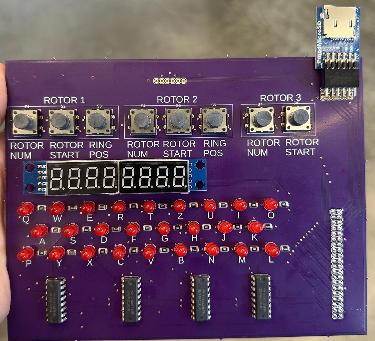
Weekly Status Reports

Nancy’s Status Report for 3/22

This past week, I worked on the microSD card implementation. I tried to test our microSD card reader with a multimeter to see what its idle voltage was (3.3V or 5V) but after doing some more research, I realized that the microSD card must be inserted in order to activate pull up resistors in the reader. So, while we waited for the microSD card to arrive, I started on the RTL of the microSD card reader, which is SPI protocol. I found a resource from MIT that implemented SPI microSD card protocol in Verilog, but it was dated for the modern microSD cards we were using. With this reference on SPI commands sent for microSD, I added additional steps in the protocol to make it compatible with our new cards. Additionally, I found a different microSD card reader that is made to operate on 3.3V and SPI mode, which would eliminate any concerns about if the reader’s I/O would need to be bumped up to 5V or down to 3.3V to interface with the FPGA. This has more pins (12 vs 6) but some of them can be tied to ground, so it is not too much of a difference.

This week, I will simulate the RTL with data that reflects how we will store the rotor encodings. Also, when the microSD cards arrive, I will see if our current microSD card reader works, and if so, I will hopefully try to synthesize with the FPGA I/O pins. Tomorrow, Tanisha and I will work on PCB routing together. Overall, we are on track and making good progress on both the embedded and RTL side.

Amelia’s Status Report for 3/22

This week I exhaustively tested the Enigma encryption that I had simulated last week and verified against the online Enigma emulator. I tested using different rotors, different rotor orders, different rotor starting positions, and different ring settings and everything worked as expected. After completely verifying the encryption I started working on integrating the encryption with the working PS2 protocol handler from last week.

My goal this week had been to integrate the keyboard inputs with the encryption algorithm and synthesize, however this turned out to be a little ambitious since I had work for other classes I needed to catch up on first. I started by writing a testbench to simulate the integration. It took quite a long time to integrate  since both components had signals on different clocks however I got it working and simulated it by Wednesday. I wrote a chip interface and synthesized later Wednesday, however I had a ton of latches in the new encryption code that I had overlooked. I had to focus on my other classes and midterms at the end of the week so my goal for next week is to fix all of these latches and synthesize the integrated PS2 and encryption logic.

Nancy’s Status Report for 3/15

This week, I mainly worked with Tanisha on the layout of the PCB. We finalized some of the arrangement of the PCB (such as moving the buttons and rotary encoder to be above the 7 segment displays) as our parts started to come in and we could get a sense for how they would fit together on top of the FPGA. Once these decisions were finalized, we were able to start thinking about how best to format our silkscreen and other aesthetic choices so that users could easily use our product and for it to be more historically accurate.

Above is our most recent PCB layout, with a single rotary encoder on top, 8 buttons to control the 8 seven segment displays, and the display underneath it. The microSD card reader pins are to the right and the lampboard is underneath the buttons. There are four shift registers to cover the many outputs of the lampboard, and the DE10 header is on the bottom right.

Additionally, Amelia and I met to discuss the plan moving forward on the RTL now that she had successfully implemented the PS/2 protocol. She also caught me up on what I had missed when I was sick on Wednesday, and we had our ethics discussion as a team after that. We decided that the most pressing issue after the PS/2 was to ensure that the microSD card protocol worked as well.

However, after the issues we had with our PS/2 keyboard (see the team status report), I started to worry that we may have the same problem with our microSD card reader, since it requires 5V. While there is a 5V source pin on the FPGA GPIO header, all of the GPIO pins are 3.3V logic, and we do not want to provide too much voltage to the pins. After looking at the Amazon reviews and description of the microSD card reader, it still seemed ambiguous if it could function with both 3.3V and 5V, as the reader does step down the 5V to 3.3V internally. I plan on testing the reader now that it has been delivered to see what the idle voltage of the MISO line is, and hopefully it is 3.3V. Otherwise, we may have to explore other ways to regulate the voltage.

Next week, I will focus on the microSD card functionality. This includes verifying that the reader will work with 3.3V so that we can finalize this on our PCB, and then I will move onto implementing SPI protocol for the microSD card in RTL. Our PCB is moving along nicely, and I will help Tanisha with the traces as needed. Overall, we are on track, especially since the keyboard issue resolved itself with Amelia’s hard work!

Amelia’s Status Report for 3/15

This week I finished my main goal of getting the PS2 protocol working and synthesized on the DE10! At the beginning of the week I debugged my own implementation of PS2, wrote and testbench and got the simulation working. However, I decided to pivot to modifying an existing PS2 protocol that I found online after realizing I was missing some of the handshaking signals in my current implementation.

I spent Tuesday debugging the online implementation and updating it to run on a DE10 (the old version was for DE2). On Wednesday, I was able to synthesize with only a few minor bugs! However, when testing with the Perixx PS2 keyboard we had ordered from Amazon, only the scan code “AA” was sent which means that the keyboard’s “Self Test Passed”. After looking at the user manual I realized that the PS2 port on DE10 was only providing 3.3V and the keyboard required 5V (oops). After looking at some PS2 reddit forums, it seemed like most people online agreed that old PS2 keyboards were compatible with PS2 ports of various FPGAs and the newer Perixx PS2 keyboards seemed to just not work.

We decided to go hunting on Facebook Marketplace for some old PS2 keyboards and Tanisha found someone selling 2 keyboards close to campus. Tanisha and I met the seller outside the CMU Police station on Friday and got two old HP PS2 keyboards for $15. The seller actually ended up refunding the cost as good luck for our capstone so it ended up being free! I went straight to lab and the FB Marketplace keyboard worked immediately! In the video below I just press a few keys on the keyboard and the scan code corresponding to that key is displayed on the FPGA’s seven segment display. 

I spent Friday and today working on the actual enigma encryption. I based my code on some of the logic in this FPGA enigma machine and hardcored the rotor settings based on the 1930 ‘Enigma I’ model  and the reflector on “Reflector B” from spring 1942. I got the encryption working in simulation today and verified my outputs with this online enigma emulator. Next week I hope to get this code synthesized with keyboard inputs and the rest of the inputs (rotor, ring, reflector) hardcoded.

This week I accomplished more than I had hoped and the RTL is coming along well! After synthesizing the encryption with the keyboard I’ll start looking into the microSD card RTL and rotary encoder FSMs. 

ps2 demo

Team Status Report for 3/15

This week the Embedded team worked on updated power considerations for the PCB, redesigned the layout to be much cleaner, ordered all relevant parts, replanned the layout over the FPGA, and continued working on the layout of the PCB.

Embedded team is currently in progress for unit testing individual parts (e.g. SD card reader, MAX7219) to confirm power considerations. The datasheet specifies a range but the FPGA GPIO pins is only able to supply 3V3 so further testing is needed to determine if output signals of these components are sending properly with a lower voltage than typical (5V). We also looked into alternate methods of powering such devices – for testing purposes – and finalized our testing plan.

For the upcoming week, Embedded team plans to complete unit testing, update layout accordingly, finish tracing the layout, and order the PCB.

This week the Verilog team worked on writing the protocol for the PS/2 keyboard. After implementing it and trying to test it, we found multiple online implementations for the same protocol to use as a guide. However, all 3 had more depth in implementation (extra acknowledges and error checks), so tried to simulate with their code (an university group from Toronto as the other two implementations were unfinished). This did not work initially because of power constraints with our PS/2 keyboard, and after some research we determined this may be because of the specific Perixx manufacturer who tied their power to 5V whereas our FPGA GPIO pins only supported 3.3V. Tanisha and Amelia sourced another PS/2 keyboard (HP manufactured) from facebook marketplace which worked with our implementation (and sustainable!).

Currently, the Verilog team is working on the encryption modules and successfully got them to simulate! The goal for this week is to synthesize and start working on the SD Card reader as that is the other component that has potential for integration issues.

As a team we received feedback on our Design Report and had a meeting to discuss improvements that need to be implemented for our final report.

Tanisha’s Status Report for 3/15

This week I worked on completing the layout of our PCB and ordering all of our parts. We ordered the rotary encoders, MAX7219 7-Segment Display, SD Card readers, and sourced the remaining miscellaneous parts (Micro SD cards, adapters, buttons, LEDs) . Due to a shortage in stock we could only order 2 rotary encoder instead of 3 so we updated our design to only include 1 rotary encoder.

Nancy and I reorganized our PCB layout to be much cleaner, more historically accurate and updated power considerations. We updated the layout of our PCB to be historically accurate to the actual Enigma machine’s lampboard (different from the standard qwerty keyboard – attached). We also adjusted spacing for 10 mil traces as a safety precaution, updated our button footprint with the new tactile button we settled on and changed the layout to float above the FPGA at a diagonal so the onboard buttons and 7-segment display can be accessed as a fallback option. The in progress PCB layout is attached below.

I worked with Amelia a little on the logic of our PS/2 protocol that she wrote and also worked on finding the solution to a setback when our current PS/2 keyboard didn’t work with the power supplied from the FPGA. Nancy and I are planning to mitigate this potential setback with the SD Card reader by testing the required power level for a measurement to be read. Accordingly, we can build in a voltage regulator to our PCB so we don’t have power issues during integration.

This week I will order remaining small parts including 100 Ohm resistors and  right angled header pins. I also plan to finalize PCB layout with updated power considerations, finish the traces and add silk screen labelling for user friendliness. Once PCB work is done, I will work on formatting and writing our MicroSD cards so they adhere to a format that is readable by our SD Card reader and hence our SPI protocol can accurately extract information.

Amelia’s Status Report for 3/8

Last week I worked on finishing up the design report. I wrote the system implementation for all of the RTL modules, designed new FSMs for the SPI and PS2 protocol, worked on design trade studies with Nancy, transcribed everything to LaTeX and created a testing plan for the RTL. I also created new block diagrams based on our updated system architecture. This week I wrote all of the RTL for the PS2 protocol, simulated it and am currently in the process of debugging.

Nancy’s Status Report for 3/8

Since the last status report, I mainly worked with Amelia on completing a lot of the writing for the design report. I specifically worked on the use-case requirements, design trade studies, the system implementation for the custom PCB, the test and validation, and the risk management.

Additionally, when finalizing the components on our PCB with Tanisha, we realized that a matrix scanning implementation of the keyboard would be overly complicated and would require many GPIO pins. I spent some time researching alternatives to keyboards, since we did not want to implement a complicated USB protocol for a USB wired keyboard. When doing more research, I found that the Altera DE10-Standard had a PS/2 port which would support a PS/2 keyboard with a much simpler protocol, so we pivoted our design back to the DE10, which allowed for one PCB that will fit on the top of the DE10. This is also what I wrote about in the design trade studies section of our report.

We initially hoped to have our PCB out for fabrication before spring break, but due to our last minute changes in design and FPGA type, this will be delayed. I will work with Tanisha on the layout this week so we can have it ordered by this week. While we wait for the PCB to be delivered, I will also work with Amelia on the RTL so that we are not wasting time, which will catch us back up to schedule. I hope to complete the PCB layout by this week and start on the implementation of some of the RTL modules.

Team Status Report for 3/8

This past week we completed our entire design report and updated our system design.

The system overhaul came about as we switched using a ribbon cable external keyboard for a PS/2 keyboard. This decision led to us switching our FPGA back to the Altera DE10 Standard as opposed to the DE0 Nano. We had initially switched to the DE0 as it had many more GPIO pins which would have been useful if we were doing a custom onboard keyboard. However, since we scrapped that in favor of the more user friendly (and optimized GPIO pin friendly) PS/2 keyboard we no longer needed those pins but rather needed the PS/2 port available on the Altera DE10 Standard FPGA. This meant we added an additional RTL module (PS/2 protocol interface) for our Verilog team and changed our PCB design for the Embedded team.

Another design change we made was using rotary encoders instead of potentiometers for our user input. We decided upon this as since we were no longer using the DE0 Nano, there weren’t any dedicated ADC pins to use and hence wasn’t any benefit to using a specifically analog input. By using a rotary encoder, it had much more user friendly interface as they are meant for comfortable user input. A big improvement was the digital pulses associated with the rotary encoder with specific pulse amounts (e.g. 24/36) as opposed to the potentiometer that had an analog continuous variable resistance change. Since our application cares more about the precise readings (e.g. which letter user is inputting), we don’t care as much about range of motion that the potentiometer offers.

This week the Embedded team will work on laying out the PCB and ordering parts and the Verilog team will work on writing the PS/2 keyboard protocol code as well as starting to synthesize it when the keyboard arrives.


Part A: Global factors

Worldwide factors that our product specification meets includes the education of a broad audience on the historical and technical significance of the Enigma machine. By providing a hands-on learning experience that is accessible by individuals of different backgrounds, contexts and levels of technological understanding. Since our solution is open source and built for educational purposes, it removes barriers to access of this knowledge and contributes to the global effort for greater STEM education efforts. By making this technology accessible beyond academic institutions, we enable individuals without access to specialized education a look into foundational cryptographic principles.


Part B: Cultural factors

We are creating this product with deep awareness of the cultural and historical significance of the Enigma machine. While the focus is an appreciation for groundbreaking technological achievement, it is also closely linked to World War II, a conflict that had profound impact on societies worldwide. Our focus is to highlight the engineering and cryptographic innovation rather than its wartime application, and ensure we approach the subject with appropriate sensitivity. To ensure a respectful and responsible presentation, we plan to include educational materials that provide a well-rounded historical perspective, recognizing both the machine’s technological advancements and the broader impact of the war. By making this accessible on a global scale, we aim to create an inclusive learning experience that allows individuals from different backgrounds to engage with the material in a meaningful and thoughtful way.


Part C: Environmental factors

With our design, we are creating a single PCB as our only custom piece of hardware, hence reducing excess electronic components and unnecessary manufacturing overhead. Additionally, our decision to use PS/2 keyboards aligns with our environmentally conscious approach as these are widely available and can be repurposed from old offices/schools/labs that have since transitioned to newer models. Finally, by emphasizing digital resources in our open-source documentation, we reduce the need for printed materials hence reducing our environmental footprint.


Part A was written by Amelia, B was written by Nancy and C was written by Tanisha.

Tanisha’s Status Report for 3/8

This week I worked on updating the PCB schematic design as we pivoted (for the final time) from using the Altera DE0 Nano standard FPGA to the Altera DE10 FPGA.

Originally I had worked on expanding our PCB design to be two separate PCBs for the DE0 Nano as the ADC pins for our potentiometer were on the underside of the FPGA and hence we split up the rotor control elements to be on separate PCBs (top layer: microSD card reader, lampboard, keyboard), (bottom layer: potentiometer, MAX7219 display, buttons).

However, when it came to researching the external keyboard, I was looking into different types of ribbon cables and found that the easiest to implement would be with a 30 pin ribbon cable connector to an FFC on the FPGA. The problem with this is we wouldn’t have enough pins on the current set of GPIO pins we were using on the FPGA which meant we’d have to incorporate a 3rd PCB to be used on the other side of the FPGA which seemed like a waste of resources (time, money, space) as it’s just wiring for the keyboard.

Nancy and I worked together to look into alternatives to this solution, and Nancy proposed we use a PS2 Keyboard which simply has a single plug to interface with the keyboard. The alternatives were either creating another plug connector on the PCB that interfaces with FPGA GPIO pins, or during research Nancy found that the Altera DE10 Standard FPGA (that we started with) that actually had an onboard PS/2 plug.

This led to the overhaul of our design as we switched back to the DE10. This led to only a single PCB instead of 2 separate ones and hence I redid the PCB schematic to be as such as attached below.

We also did some hands on testing with the FPGAs to ensure we had the right pitch/pin sizes for our headers and were pleased that we can just use standard headers (as this information was not provided in the user manual somehow).

I also began laying out this PCB design – attached is a screenshot of the in progress layout with descriptive tags.

I also worked on the Design Report and created our new Bill of Materials which is clearly updated with all of our finalized parts according to the new PCB design.

This week I plan to complete the layout of our PCB, send it for ordering, and order all our individual parts so it has enough lead time to get here alongside the PCB manufactoring process. This is slightly off schedule our original plan, however this was due to the frequent switching of design and parts we were planning on using (potentiometers -> rotary encoders, #headers, pcb keyboard -> external keyboard), and hence was a wiser choice to put off ordering till now.