Last week I worked on finishing up the design report. I wrote the system implementation for all of the RTL modules, designed new FSMs for the SPI and PS2 protocol, worked on design trade studies with Nancy, transcribed everything to LaTeX and created a testing plan for the RTL. I also created new block diagrams based on our updated system architecture. This week I wrote all of the RTL for the PS2 protocol, simulated it and am currently in the process of debugging.
Category: Status Reports
Nancy’s Status Report for 3/8
Since the last status report, I mainly worked with Amelia on completing a lot of the writing for the design report. I specifically worked on the use-case requirements, design trade studies, the system implementation for the custom PCB, the test and validation, and the risk management.
Additionally, when finalizing the components on our PCB with Tanisha, we realized that a matrix scanning implementation of the keyboard would be overly complicated and would require many GPIO pins. I spent some time researching alternatives to keyboards, since we did not want to implement a complicated USB protocol for a USB wired keyboard. When doing more research, I found that the Altera DE10-Standard had a PS/2 port which would support a PS/2 keyboard with a much simpler protocol, so we pivoted our design back to the DE10, which allowed for one PCB that will fit on the top of the DE10. This is also what I wrote about in the design trade studies section of our report.
We initially hoped to have our PCB out for fabrication before spring break, but due to our last minute changes in design and FPGA type, this will be delayed. I will work with Tanisha on the layout this week so we can have it ordered by this week. While we wait for the PCB to be delivered, I will also work with Amelia on the RTL so that we are not wasting time, which will catch us back up to schedule. I hope to complete the PCB layout by this week and start on the implementation of some of the RTL modules.
Team Status Report for 3/8
This past week we completed our entire design report and updated our system design.
The system overhaul came about as we switched using a ribbon cable external keyboard for a PS/2 keyboard. This decision led to us switching our FPGA back to the Altera DE10 Standard as opposed to the DE0 Nano. We had initially switched to the DE0 as it had many more GPIO pins which would have been useful if we were doing a custom onboard keyboard. However, since we scrapped that in favor of the more user friendly (and optimized GPIO pin friendly) PS/2 keyboard we no longer needed those pins but rather needed the PS/2 port available on the Altera DE10 Standard FPGA. This meant we added an additional RTL module (PS/2 protocol interface) for our Verilog team and changed our PCB design for the Embedded team.
Another design change we made was using rotary encoders instead of potentiometers for our user input. We decided upon this as since we were no longer using the DE0 Nano, there weren’t any dedicated ADC pins to use and hence wasn’t any benefit to using a specifically analog input. By using a rotary encoder, it had much more user friendly interface as they are meant for comfortable user input. A big improvement was the digital pulses associated with the rotary encoder with specific pulse amounts (e.g. 24/36) as opposed to the potentiometer that had an analog continuous variable resistance change. Since our application cares more about the precise readings (e.g. which letter user is inputting), we don’t care as much about range of motion that the potentiometer offers.
This week the Embedded team will work on laying out the PCB and ordering parts and the Verilog team will work on writing the PS/2 keyboard protocol code as well as starting to synthesize it when the keyboard arrives.
Part A: Global factors
Worldwide factors that our product specification meets includes the education of a broad audience on the historical and technical significance of the Enigma machine. By providing a hands-on learning experience that is accessible by individuals of different backgrounds, contexts and levels of technological understanding. Since our solution is open source and built for educational purposes, it removes barriers to access of this knowledge and contributes to the global effort for greater STEM education efforts. By making this technology accessible beyond academic institutions, we enable individuals without access to specialized education a look into foundational cryptographic principles.
Part B: Cultural factors
We are creating this product with deep awareness of the cultural and historical significance of the Enigma machine. While the focus is an appreciation for groundbreaking technological achievement, it is also closely linked to World War II, a conflict that had profound impact on societies worldwide. Our focus is to highlight the engineering and cryptographic innovation rather than its wartime application, and ensure we approach the subject with appropriate sensitivity. To ensure a respectful and responsible presentation, we plan to include educational materials that provide a well-rounded historical perspective, recognizing both the machine’s technological advancements and the broader impact of the war. By making this accessible on a global scale, we aim to create an inclusive learning experience that allows individuals from different backgrounds to engage with the material in a meaningful and thoughtful way.
Part C: Environmental factors
With our design, we are creating a single PCB as our only custom piece of hardware, hence reducing excess electronic components and unnecessary manufacturing overhead. Additionally, our decision to use PS/2 keyboards aligns with our environmentally conscious approach as these are widely available and can be repurposed from old offices/schools/labs that have since transitioned to newer models. Finally, by emphasizing digital resources in our open-source documentation, we reduce the need for printed materials hence reducing our environmental footprint.
Part A was written by Amelia, B was written by Nancy and C was written by Tanisha.
Tanisha’s Status Report for 3/8
This week I worked on updating the PCB schematic design as we pivoted (for the final time) from using the Altera DE0 Nano standard FPGA to the Altera DE10 FPGA.
Originally I had worked on expanding our PCB design to be two separate PCBs for the DE0 Nano as the ADC pins for our potentiometer were on the underside of the FPGA and hence we split up the rotor control elements to be on separate PCBs (top layer: microSD card reader, lampboard, keyboard), (bottom layer: potentiometer, MAX7219 display, buttons).
However, when it came to researching the external keyboard, I was looking into different types of ribbon cables and found that the easiest to implement would be with a 30 pin ribbon cable connector to an FFC on the FPGA. The problem with this is we wouldn’t have enough pins on the current set of GPIO pins we were using on the FPGA which meant we’d have to incorporate a 3rd PCB to be used on the other side of the FPGA which seemed like a waste of resources (time, money, space) as it’s just wiring for the keyboard.
Nancy and I worked together to look into alternatives to this solution, and Nancy proposed we use a PS2 Keyboard which simply has a single plug to interface with the keyboard. The alternatives were either creating another plug connector on the PCB that interfaces with FPGA GPIO pins, or during research Nancy found that the Altera DE10 Standard FPGA (that we started with) that actually had an onboard PS/2 plug.
This led to the overhaul of our design as we switched back to the DE10. This led to only a single PCB instead of 2 separate ones and hence I redid the PCB schematic to be as such as attached below.
We also did some hands on testing with the FPGAs to ensure we had the right pitch/pin sizes for our headers and were pleased that we can just use standard headers (as this information was not provided in the user manual somehow).
I also began laying out this PCB design – attached is a screenshot of the in progress layout with descriptive tags.
I also worked on the Design Report and created our new Bill of Materials which is clearly updated with all of our finalized parts according to the new PCB design.
This week I plan to complete the layout of our PCB, send it for ordering, and order all our individual parts so it has enough lead time to get here alongside the PCB manufactoring process. This is slightly off schedule our original plan, however this was due to the frequent switching of design and parts we were planning on using (potentiometers -> rotary encoders, #headers, pcb keyboard -> external keyboard), and hence was a wiser choice to put off ordering till now.
Nancy’s Status Report for 2/22
In the beginning of the week, I finalized the design presentation, especially making sure that our use case requirements were quantifiable and translated into quantifiable design requirements. Later, I worked on the design report, adding more to the introduction and use case requirements sections. Most of this was elaborating on how our use case and its social/economic/historical implications leads to our quantitative requirements.
I also worked with Tanisha on finalizing our PCB schematic. While reading the De0-Nano datasheet, I saw that we had overlooked how the ADC pins are on the bottom of the FPGA, unlike the 2 2×20 GPIO pins. However, the ADC pins are also only accompanied by 13 GPIO pins, so it would not be possible to put all of our I/O on the bottom pins. So, I began exploring how to split up our PCB into 2, with the rotor functionality on the bottom pins where the potentiometers would be (which would need the ADC pins), and the lampboard/SD card/keyboard using the top pins. Additionally, I spent some time looking for the footprint for the FPGA, but I could only find a Fusion-compatible version for the bottom pins. This was a concern since we wanted the PCB to fit perfectly over the top pins on the FPGA and we want the spacing between the two 2×20 headers to be accurate. However, since we can move some functionality to the bottom pins, we only have to use one of the 2×20 headers, eliminating this concern.
Finally, I also researched into interfacing with the ADC and SD card reader through the FPGA. I found two Intel IP cores that work with Quartus that could be helpful — the ADC and SPI cores.
In order to stay on schedule, Tanisha and I need to finalize the PCB schematic and layout before spring break, which will be a good amount of work but doable with us both. This week, I hope to finish this so we can order the PCB over break, and also continue to edit the design report once we receive feedback on our presentation.
Tanisha’s Status Report for 2/22
This week I worked on preparing for the design presentation as it was my turn to present. I felt prepared and confident in my slides and content and thought it went well overall. I also continued to fix things on our draft schematic. Since we changed our FPGA, I picked up our new one this week and have been adjusting the schematic to make sure the PCB size and layout matches the DE0 Nano layout and pins. This was a struggle before we had our hands on the physical FPGA as there seemed to be multiple versions of the DE0 Nano and we couldn’t tell which layout/datasheet we should be adhering to. I aim to have an updated schematic done this week so we can get the layout done as soon as possible and send it for fabrication over spring break and continue stay on schedule. If time permits this week, I also hope to return to my external keyboard research so if that arrives after break I can start to mess around with the actual connections and test the ribbon connector. I anticipate this to take a while as it is hardware I am unfamiliar with and tricky hardware issues may take some time.
Team Status Report for 2/22
This week we worked on finishing up the Design Presentation slides and finalizing our quantitative use case requirements, trade offs, and testing and verification plan. We also picked up our new FPGA (moved from DE10 to DE0). Due to our design changes from last week, we updated the schedule, see below.
The most significant risk that our project could face is the custom PCB not being completed in time. However, since we have decided to use a local supplier instead of one from China, the lead time is significantly reduced and we can afford to take all the necessary steps and time to ensure that our custom PCB will hopefully be successful. Since a big design change from last week, this week we worked on fleshing out the design of our peripherals. One big change was deciding on using a microSD card reader on the PCB rather than using the reader on the FPGA. This had been our original plan when we were still using an Arduino.
Amelia’s Status Report for 2/22
This week I spent most of my time working on the design report. I wrote the Abstract, Introduction, Use-case Requirements, Architecture and/or Principle of Operation, Design Requirements, Design Trade Studies, and some of the Test and Validation and Project Management sections. We just need to finish the System Implementation and Test and Validation sections once our custom PCB is finalized. I carried most of the writing for the design report because Tanisha and Nancy are occupied with making the schematic and layout for the custom PCB. I also iterated on the FMSs for the rotors and Enigma keypress from last week to removed some unnecessary reset states. — see updated FSMs below. Next week, I will finish up the design report and start planning out my Enigma modules before spring break.
Team’s Status Report for 2/15
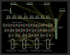
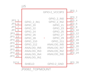
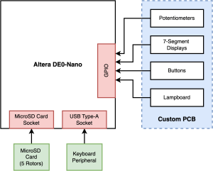
This week we faced larger design changes based on the feedback from our Proposal presentation. This led to an updated design where we decided to adjust the number of modules in order to stick to our primary use case of historical accuracy. Taking the advice and criticisms of our peers and faculty, we incorporated it into our iterative design. This was the determining factor in us deciding to move the functionality from our Arduino to the FPGA. For example, moving the rotor functionality to the FPGA board and by connecting all our external peripherals directly to the FPGA I/O pins. This also included switching our FPGA from the Altera DE10 Standard to the Altera DE0 Nano as the number of pins jumped exponentially from 40 to 80.
Part A: Public Health, Safety, and Welfare Considerations
Our FPGA-based Enigma machine replica is designed to be a safe and historically accurate educational tool for classrooms and museums. By using an FPGA instead of fragile electromechanical components, we eliminate risks associated with mechanical wear, electrical faults, and high-voltage circuits, ensuring safe hands-on use. The modular, lightweight design simplifies transportation and setup, making it easy for educators to integrate into various learning environments without specialized technical expertise. The product will be built with durable, non-conductive materials to prevent electrical hazards, with all components carefully selected to comply with safety regulations.
To ensure quality and reliability, we are sourcing PCBs domestically, maintaining high manufacturing standards and supply chain consistency. The result is a durable and practical tool that enhances historical education while prioritizing safety and ease of use.
Part B: Social Considerations
Our project is a historically accurate yet modernized Enigma machine designed to serve as an interactive educational tool. By offering a hands-on learning experience, it fosters an appreciation for cryptography, wartime history, and the evolution of computing. Its open-source design encourages collaboration among educators, students, and enthusiasts from diverse backgrounds.
With a focus on modularity and ease of assembly, the device is practical for use in museums, classrooms, and historical institutions. By making history interactive, we connect historical cryptography with modern cybersecurity discussions, providing value to both history enthusiasts and technology professionals. This project contributes to the broader effort of preserving and communicating historical knowledge in an engaging and meaningful way.
Part C: Economic Considerations
Our project is designed to be cost-effective and sustainable. By remaining open-source, we eliminate licensing and proprietary hardware costs, making it more feasible for institutions with limited budgets. Using an FPGA preserves the logic of the original Enigma machine while reducing maintenance needs compared to mechanical alternatives. The modular design further extends the product’s lifespan by allowing individual components to be replaced as needed.
Sourcing PCBs domestically ensures consistent quality, minimizes supply chain risks, and supports U.S. manufacturing. These choices balance historical accuracy with economic feasibility, ensuring that our Enigma machine replica remains a practical and valuable tool for education and historical preservation.
Part A was written by Nancy, B was written by Amelia and C was written by Tanisha.
Amelia’s Status Report for 2/15
This week I mostly worked on designing our finite state machines for the rotor settings and for the keyboard (see below). I also redesigned the top layer view (see below) of our schematic (with potentiometers) after getting feedback from course instructors who advised that we should include a turning rotor mechanism (we decided in the form of potentiometers) to help mimic the look and feel of the original Enigma machine. I also redesigned our system block diagram (see below) by removing the Arduino after receiving feedback from our proposal. Now our design only consists of the FPGA, custom PCB, and keyboard peripheral. I also researched the Altera DE0 Nano board as a replacement for the Altera DE10 due to the increased number of pins we’ll need since removing the Arduino from the system. Lastly, I worked on the design presentation slides.
Due to our redesign, I did not research UART like I had mentioned last week because UART is no longer needed since removing the Arduino. Next week I’ll work on finalizing the signals and modules for RTL encoding. Next week I will also likely spend quite a bit of time on the Design Report — this is because Nancy and Tanisha are working hard to finish the custom PCB to send to the fab before spring break.