This week I worked on updating the PCB schematic design as we pivoted (for the final time) from using the Altera DE0 Nano standard FPGA to the Altera DE10 FPGA.
Originally I had worked on expanding our PCB design to be two separate PCBs for the DE0 Nano as the ADC pins for our potentiometer were on the underside of the FPGA and hence we split up the rotor control elements to be on separate PCBs (top layer: microSD card reader, lampboard, keyboard), (bottom layer: potentiometer, MAX7219 display, buttons).
However, when it came to researching the external keyboard, I was looking into different types of ribbon cables and found that the easiest to implement would be with a 30 pin ribbon cable connector to an FFC on the FPGA. The problem with this is we wouldn’t have enough pins on the current set of GPIO pins we were using on the FPGA which meant we’d have to incorporate a 3rd PCB to be used on the other side of the FPGA which seemed like a waste of resources (time, money, space) as it’s just wiring for the keyboard.
Nancy and I worked together to look into alternatives to this solution, and Nancy proposed we use a PS2 Keyboard which simply has a single plug to interface with the keyboard. The alternatives were either creating another plug connector on the PCB that interfaces with FPGA GPIO pins, or during research Nancy found that the Altera DE10 Standard FPGA (that we started with) that actually had an onboard PS/2 plug.
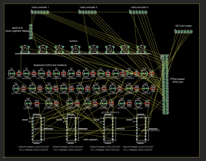
This led to the overhaul of our design as we switched back to the DE10. This led to only a single PCB instead of 2 separate ones and hence I redid the PCB schematic to be as such as attached below.
We also did some hands on testing with the FPGAs to ensure we had the right pitch/pin sizes for our headers and were pleased that we can just use standard headers (as this information was not provided in the user manual somehow).

I also began laying out this PCB design – attached is a screenshot of the in progress layout with descriptive tags.
I also worked on the Design Report and created our new Bill of Materials which is clearly updated with all of our finalized parts according to the new PCB design.

This week I plan to complete the layout of our PCB, send it for ordering, and order all our individual parts so it has enough lead time to get here alongside the PCB manufactoring process. This is slightly off schedule our original plan, however this was due to the frequent switching of design and parts we were planning on using (potentiometers -> rotary encoders, #headers, pcb keyboard -> external keyboard), and hence was a wiser choice to put off ordering till now.