Andrew’s Status Report for 4/27

Personal tasks of this week:

Task: Entire Schematics and PCB Layout

Definition: As the final pcb was due for manufacturing, the entire pcb schematic and layout needed to be finished from the entire design.

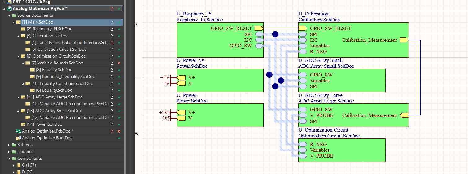
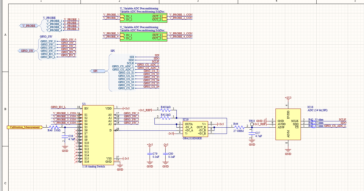
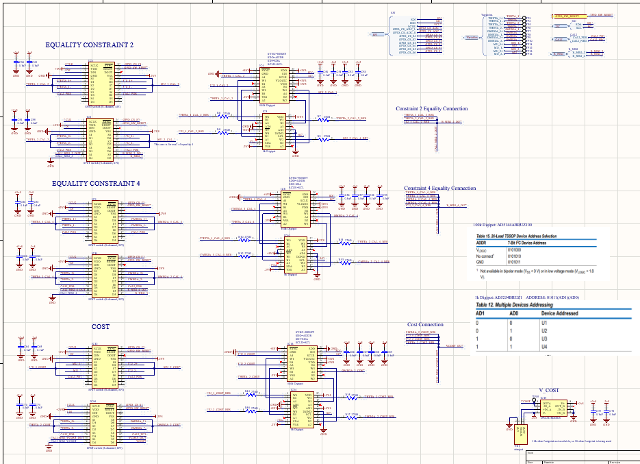
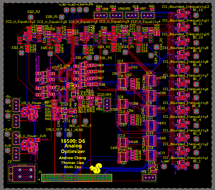
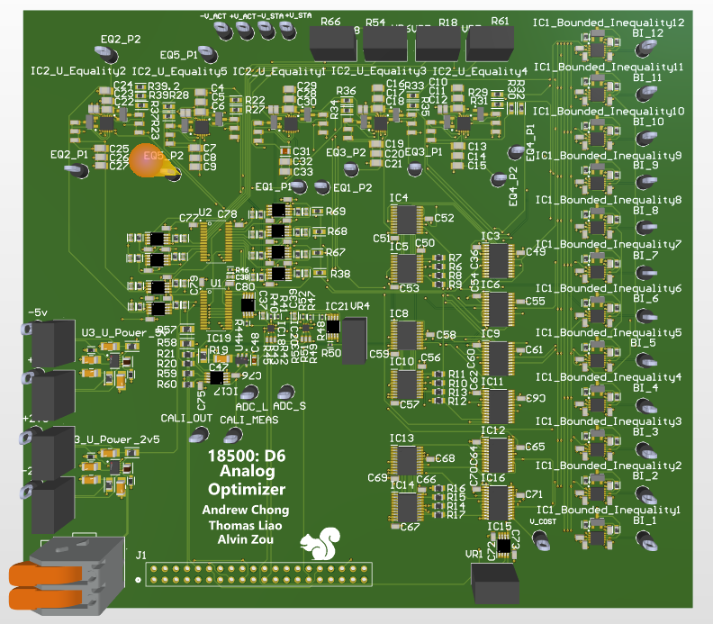
Completion: The task is completed. Thomas and I were able to finalize all aspects of the schematics first to ensure that the pcb will work. Thomas was a huge help in figuring out resistances, capacitances, and general wiring for the ICs. Afterwards, the entire layout was also completed. Here is the 2d and 3d view of the layout in Altium. Since the schematics are too large to view on one page, here is a link to the schematics: https://drive.google.com/file/d/1xAiFV6w-DaRna5lD9I2hjO9rPJXy43xM/view?usp=sharing

Next Steps:

There are no next steps on my end.

Overall progress assessment:

My progress is completed , but the overall progress of the team is behind schedule, as we need to manually reflow the pcb instead of getting it assembled, since the manufacture time would have been too long.

Andrew’s Status Report for April 20

Personal tasks of this week:

Task: Finalize circuit design and layout

Definition: Finalize the design of the circuit and the layout of the PCB so it can be ordered.

Completion: The task is partially completed. All of the schematics are completed and verified with LTSpice to work. Furthermore, we designed and implemented the digipot calibration method, as well as the protocool we will be using for the pcb. As for layout, there has been some significant progress in figuring out the majority of the connections, but the final layout still needs to be completed.

Next Steps:

My next step is to finish the layout of the PCB

Overall progress assessment:

My progress is somewhat behind schedule, because the PCB is not yet ready to be ordered.

Learning to use new tools:

A new tool I had to learn was LTSpice, which is a circuit simulation software for circuit analysis and simulation. I learned how to use it by looking at tutorials to figure out what was going on and import parts, then figured out the rest from there while looking up specific tools like simulation up.

Team Status Report of April 6

Overall progress:

We were able to fix the vast majority of the issues that we ran into implementing Sergey’s solver. Furthermore, we were able to create a full scale simulation of the swingup problem both in SLP simulation and LTSpice circuit simulation. In both cases, we were able to verify that the solutions work.

Significant risks and risk management:

Risk:  While the circuit seems to work properly, we still need to properly identify what kinds of issues arise in the physically circuit

Description: We were able to predict much of the behavior of the “real world” circuit by using the components specified in the BOM. However, the actual behavior of the circuit will obviously be different

Severity: If the inaccuracies of the physical pcb are not properly accounted for, the circuit can have a variety of errors, including non-convergence and solutions with high error.

Resolution: We are currently modeling the behavior of some of these real-world effects as electrical components. For example, we have capacitors on the op amps that do not exist in the theoretical formulation, but exist in the real world analogue due to the parasitic capacitances. However, there are many more places where these issues can occur. The largest source of error compared to the circuit is the transition from resistors to linpots.

Changes to the existing design:

There are currently no significant changes to the existing design. However, depending on the root cause of the inaccuracies, we might change the design to fix it.

Changes to the project schedule:

Similarly, there are currently no significant changes to the project schedule. We aim to order the PCB as early as possible.

Andrew’s Status Report for Apr. 6

Personal tasks of this week:

Task: Resolve issues with circuit simulation and test on swingup problem

Definition: To ensure that the circuit will work on the current swingup problem that we are trying to solve, a full scale simulation of that optimization problem must be created and tested.

Completion: The task is completed.  We were able to create a formulation of the 6 variable swingup problem in terms of the constraints. Thomas was able to create an automated method of calculating the resistances needed for each of the constraints on excel. Using this, we were able to very simply create the full contraints of our circuit. To verify that the solution works, we tried the first, last, and a random middle problem to optimizer. For all of the situations, the majority of the solutions were around 0.5% of the optimal solution, with one variable being around 2.5% of the solution. We also did a voltage sweep on the cost function voltage to verify that the previously identified “sweet spot” was the same for all of the problems.


Next Steps:

Now that the current optimization problem is verified to be correct, the pcb must be created and manufactured as soon as possible.


Verification & Validation:

As the circuit simulation is completed, we can now perform tests to gauge its accuracy on the pcb. Namely, we can run the test suite T3 as we defined in our report.

A manufactured PCB that implements the analog QP solver

We will run the test with three different starting positions to verify the correctness of the solver.

Overall progress assessment:

My progress is on-schedule, as all of my tasks this week have been completed.

Andrew’s Status Report for Mar 30

Personal tasks of this week:

Task: Test and resolve circuit issues in simulation

Definition: Work with Thomas to test representative LP problems on the analog circuit simulation to identify and fix issues that prevents it from converging to the correct solution. In particular, test with LPs that have non-zero bias terms in linear equality constraints, which has previously been problematic.

Completion: The task is completed. We have done extensive analysis and experiments in order to determine the cause of the issue. Furthermore, we have resolved all of the remaining issues with Sergey’s formulation as well.

Here is the sheet with all of our experiments: Experiments

Here are some screenshots of some of our successful simulations:


DC voltage sweep on optimal cost voltage

Success on new optimization Circuit

Next Steps:

My next step is to test the circuit for more complex optimization circuits in order to make sure that the circuit formulation method is sound, then finally try this on our pendulum LP circuit. I will also translate these circuits schematics into altium to begin pcb design.

Overall progress assessment:

My progress is on-schedule, as all of my tasks this week have been completed.

Andrew’s Status Report for March 23

Personal tasks of this week:

Task: Circuit Simulation:

Definition:  While the previous issues with Sergey’s thesis were resolved, the full scale circuit simulation must be made and tested using LTSpice.

Completion: The task is not completed :’)) . Iturns out that Sergey’s formulation of his problem introduces many issues when actually trying to solve a more general problem than the very specific problem that he formulated for his thesis.

To test the validity of the approach, we first began with creating a simple 6 variable optimization problem for the circuit primitives to solve.

The problem is as follows:

Linear Cost:  th_1+2th_2+3w_1+4w_2+5u_1+6u_2

Equality Constraints:  th_1+th_2+w_1+w_2+u_1+u_2 = 20

equality constraint: 2th_1+2th_2+w_1+w_2+u_1+3u_2 = 30

equality constraint: 3th_1+1th_2+2w_1+2w_2+2u_1+1u_2 = 40

equality constraint: 1th_1+3th_2+1w_1+3w_2+1u_1+2u_2 = 50

The largest problem that we figured out is that the circuit that solves the optimization problem does not properly converge. Through much testing, we were able to find many more issues with the current formulation being realized. In the end, we were able to get the circuit to converge to the proper voltages in less than a milisecond, but we were not able to get the circuit to converge to the correct values when adding the bias voltages for the equality constraint.

We also did some further experiments regarding the negative voltage on the linear cost to see how it converges as well.

Next Steps:The next steps is to diagnose and fix these further issues we found with Sergey’s formulation.

Overall progress assessment:

My progress is behind-schedule, as we have found more issues with the practical formulation of Sergey’s thesis.

Team Status Report for March 16

Significant risks and risk management:

Risk: The analog circuit as described by Sergey’s Thesis cannot be realized.

Definition: Through some more research and implementing his circuits through simulation, we were able to determine that the constraint primitives are not able to be realized for our optimization problem. Specifically, for the equality constraint, the theoretical formulation assumed infinite op amp rail voltages and the quadratic costs  could not properly be realized without first solving a linear programming problem.

Severity: The severity is very high. If this is not able to be resolved, our circuit will fail to converge.

Resolution:  We were able to resolve both of these issues. For the inequality, we reduced the operating voltage by 10x, so that the maximum voltage that we expect is within the rails of the op amp. As for the costs, we realized that we could not implement these quadratic costs for SQP without first solving a SLP (sequential linear programming), so we decided to compromise and solve our optimization problems using an SLP, using linear costs

Current progress:

We have resolved the issues regarding the constraints

Changes to the existing design:

We have modified our problem formulation from SQP to SLP, modified the constraints to account for op amp rail voltages, and slightly descoped the optimization problem.

Changes to the project schedule:

Similarly, there are no significant changes to the project schedule, we are a bit behind schedule with pcb ordering though.

Andrew’s Status Report for March 16

Personal tasks of this week:

Task: Circuit Simulation:

Definition:  According the Sergey’s thesis, the theoretical circuit primitives were found to model the mathematical constraint. However, the circuits need to be modified to realize the theoretical circuit, as it contains ideal circuits that don’t exist in the real world.

Completion: The task is completed. Analyzing the issues from Sergey’s thesis from last week, we were able to solve all of the issues we were facing. In regards to the equality constraint, we realized that the theoretical formulation of the constraint was correct, but did not take into account that the op-amp rail voltages are not infinite :/ As a result, if the voltages in the realized simulation end up maxing out at the rails, the circuit would continue to oscillate and never converge. To fix this, we realized that we can scale down our operating voltage from -100 mV – 100 mV, which was used my Sergey, to -10mV – 10mV. As a result, in our simulations, we can observe that the voltages properly converge. All of the simulations now are verified using the models of the finalized BOM.

Furthermore, the constraints were abstracted into components in LTSpice to make simulation much simpler and less prone to errors.

The inequality constraints were based on an op-amp clamp. Simply changing the direction of the diode will change the direction of the op-amp. Chaining two of them together can create a bounded clamp.

After slightly descoping the project, here is the finalized BOM. Now, even when considering the more expensive, but reliable option, PCBWAY, we are within the allocated budget for the project.


Next Steps:

The next steps is to create full scale simulation of the optimization circuit using our currently verified and abstracted constraints. Considering that we have slightly descoped the optimization problem to ensure that the final demo will work, we are now on budget as well.

Overall progress assessment:

My progress is slightly behind-schedule, as we have resolved all of the current issues with the circuit, but because of that, are behind in the PCB design and fabrication.

Andrew’s Status Report for March 2

Personal tasks of this week:

Task: Preliminary Circuit Simulation:

Definition:  According the Sergey’s thesis, the theoretical circuit primitives were found to model the mathematical constraint. However, the circuits need to be modified to realize the theoretical circuit, as it contains ideal circuits that don’t exist in the real world.

Completion: The task is partially completed. Further research was done in order to finalize the components that would be used. In particular, a preliminary BOM of the PCB was created:

Item Description Quantity Cost Total
OPA4376 buffer op-amp 4 3.62 14.48
OPA2328 high bandwidth op-amp 26 3.18 82.68
AD5144ABRUZ100 100k digipot (I2C) 16 8.18 130.88
AD5254BRUZ1 1k digipot (I2C) 16 8.59 137.44
ADS7056 ADC (14-bit) 1 5.32 5.32
ADG732 1:32 Analog mux 1 14.41 14.41
MCP47CVD22 DAC (12-bit, 2-channel) 6 3.23 19.38
TCA9548A i2c multiplexer (8-channel) 3 1.19 3.57
ADG734BRUZ-REEL7 switches (4-channel) 19 4.23 80.37
BAS70-04S diode (2×2) 8 0.54 4.32

Furthermore, while we found significant issues with the realized formulation of Sergey’s thesis, we were able to create and simulate the realized constraints in LT Spice. The behavior of each constraint was verified and now only the simple optimization problem needs to be created.


Next Steps:

The next steps are to first create and verify the simple optimization problem, and then scale to the full problem once we are able to resolve the issues and concerns we have with Sergey’s thesis.

Overall progress assessment:

My progress is slightly behind-schedule, as we needed to address issues regarding Sergey’s thesis, but we have resolved the majority of issues regarding it.


Andrew’s Status Report for Feb 24

Personal tasks of this week:

Task: Preliminary Circuit Simulation:

Definition:  According the Sergey’s thesis, the theoretical circuit primitives were found to model the mathematical constraint. However, the circuits need to be modified to realize the theoretical circuit, as it contains ideal circuits that don’t exist in the real world.

Completion: The task is partially completed.  The circuit was researched and equivalent components from the thesis that can be sourced now were found for each component.  The circuit was attempted first in PSpice, but decided to transition into using LTSpice, as we realized the speed of learning and prototyping ability of LTSpice was much more important given our time constraints compared to the features available on PSpice. A basic schematic was built for each primitive, but has not been tested extensively for the simple optimization circuit

Next Steps:

The next steps are to use PSpice to create the simulation of the simple optimization circuit and verify if the minimum energy state converges to the expected solution.

Overall progress assessment:

My progress is slightly behind-schedule, as I still need to finish up the optimization circuit, but it should not be that difficult to catch up, as the components have already been selected and imported.