With the complete PCB design, we removed some of the planned backup plans since they were not feasible. The big one is that we were planning on leaving some extra DNP pads for more green photodiodes in case our photodiodes are not strong enough. However, there is slightly more risk now since we had to remove this to make layout work.
We noticed that the FPGA board lists some pins as clock pins. The Datasheet does not describe what this means. This is 2 pins from the FTDI chip and the 2 IR laser controlling pins. If this ends up being an issue, we can accommodate it by using an interface with the FTDI chip that does not use those pins (fast serial) and by testing that the IR laser pins operate at high enough speed.
Design Changes
Our PCB will be much smaller than the FPGA board rather than a copy of it. This is because the parts fit on a much smaller footprint, and making it smaller makes buttons and LEDs on the FPGA board accessible, and it will be easier to make sure the boards fit together.
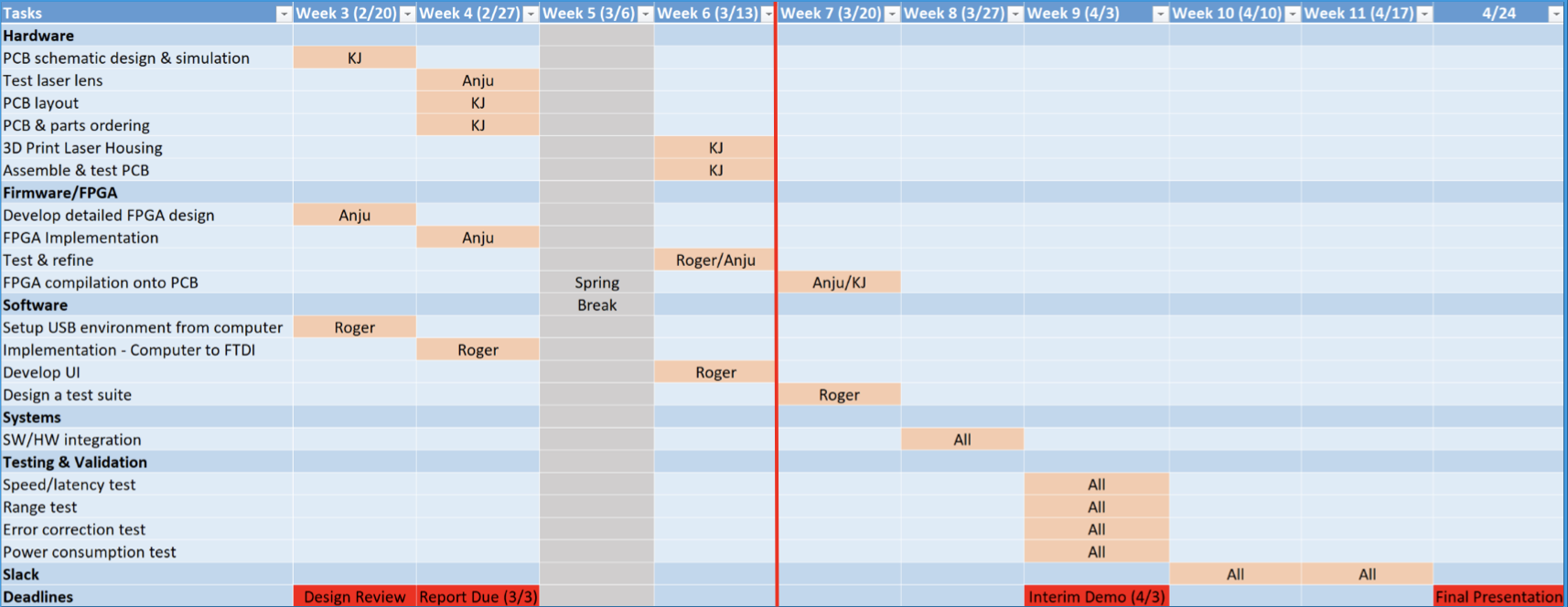
Updated Schedule
In terms of schedule, software developments (Roger) were impacted by inability to develop software for hardware that had not been fully finalized. We have instead begun working on sender implementation as well as a preliminary UI interface to input text files for sending in order to be productive within the schedule constraints.
No changes have been made to the hardware schedule as the PCB and part orders went out on time
Progress
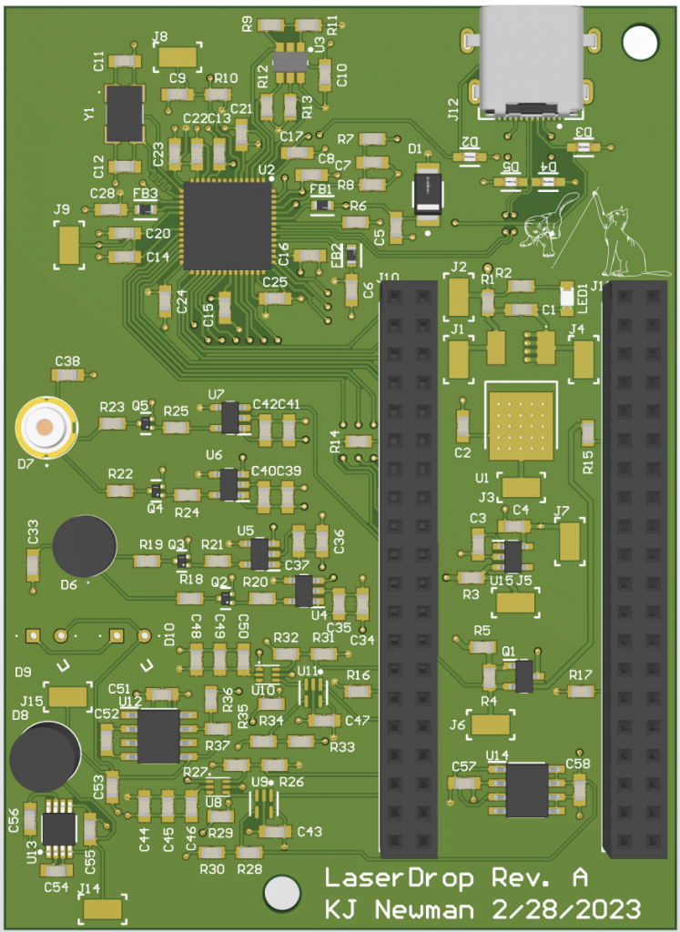
PCB design is complete! Our PCB and all components for it have been ordered and should arrive by the time we return from spring break.
Sender implementation for the bitwise hamming encoding of files has been implemented
We completed our design report paper
New Tools
We will need to learn to use FT_PROG to program the EEPROM to save settings for our FTDI chip
We will need to experimentally identify the best way to view the infrared laser for debugging and testing. We currently plan on using the front-facing camera from our phones, as they typically do not have IR-cut filters. However, this may not work. In that case, we will need to learn to use an IR camera to measure it.
This week, I completed our PCB design. I did our layout and it passed all DFM checks. It is currently in fabrication at JLCPCB and expected to arrive before class resumes after winter break.
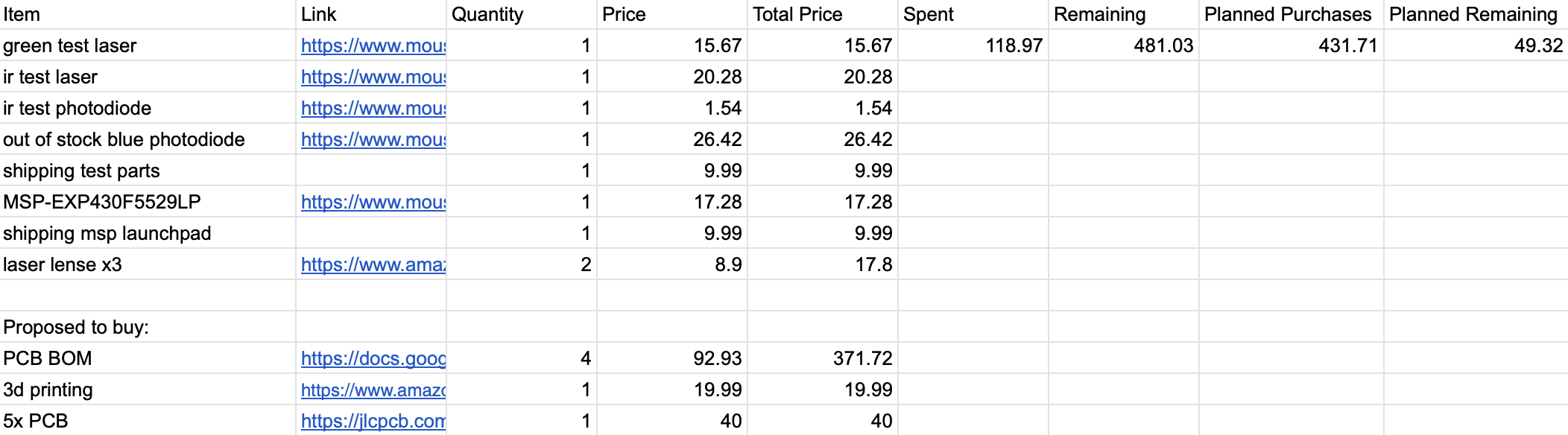
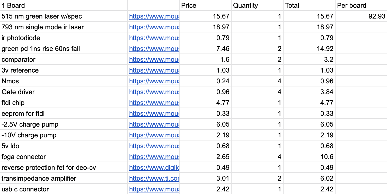
I ordered all parts to make our PCB. Our only expected expense that has not been purchased yet is 3d printer filament. This has 1 day shipping so can be purchased later. Setting up our part orders was a bit complex because I wanted to order with bulk discounts where possible and buy extra components in case we need them, but we are running a little close to the $600 budget. I ultimately ordered enough active components for 3 boards and numbers of resistors and capacitors to get bulk discounts.
I wrote my parts of the design report. This was a lot of work to do in parallel with finishing and ordering the PCB, but we managed to finish it.
Schedule
My parts are on schedule. I planned on having the pcb ordered before spring break and set to arrive after spring break, and it should be here by then.
Deliverables
For next week, I plan to have 2 PCBs fully assembled and ready for use. This should be achievable, since all of our parts will have arrived before the beginning of the week.
This week, I completed the schematic for our custom PCB. This included adding as many backup plans to the board as possible so it will still work even if I made some mistakes and some parts do not work as expected. I also had the schematic reviewed by both of my teammates and several other people to verify that I did not make any mistakes. This included doing calculations to ensure that the board will meet all timing requirements and finding an example board using our FTDI chip, since it is fairly complicated.
I completed our budget this week. This included specifying the exact BOM of the board, as well as figuring out how much extra of each part to order, and how best to acquire passive components. We are buying all parts we need, and purchasing as much as we can on multiples of 10 and 100 to get discounts. This means that our order of passives costs $0.01 more than buying enough for 2 boards, and it has over 100 more extra parts. The budget also includes all of our prototyping parts, 3d printing, shipping, a stencil, and everything else we will spend on. We will have $80 left over for anything that comes up later.
Schedule
My work is on schedule. I wanted to complete the schematic this week, and I had it done early in the week. We also tested the lens this week, which is ahead of schedule. I am confident we will be able to order parts and the PCB before Spring break, as I have a week for layout.
Deliverables
I hope to complete our layout for our pcb in the next week. This way we can order it next week and have it in hand when we return from Spring break.
One risk is that the PCB will not be capable of the speeds we want. We do not have tremendous experience with high speed routing, so it is possible that the layout will cause issues.
We will mitigate this by doing a lot of research into high speed routing before doing layout work. Additionally, we will keep high speed traces very short.
Component availability between early stage of design and component ordering
We plan on ordering components as soon as schematic work is done to mitigate this. Additionally, we are ordering some extremely low availability components already.
Design Changes
We switched to using a FTDI to Fast Serial chip because the FIFO chips output a 60 MHz clock, which will cause issues both due to parasitic capacitance and inductance and the FPGA clock only being 50 MHz. This allows us to run the clock between FPGA and FTDI chip from 183 Hz to 12 MHz.
We switched to powering the board over USB Power Delivery. This allows us to request a voltage and receive it from the laptop over USB (in our case 9V). This removes the need for a boost converter on the board.
We will now power the FPGA board through the custom PCB, as this can be done with a diode reverse protecting the board.
We switched to a different IR laser diode because the prior one had a very odd configuration internally between its internal laser diode and photodiode that made it difficult to power.
We switched FPGA boards. We had acquired the wrong one (DE10) and switched to DE0-CV.
We will now use laser lenses that are threaded. This will enable us to screw the lens in and out to change focus without needing to create a new 3d printed housing for every focal length change, which should reduce the number of 3d prints we need to only 1.
We switched to using a custom UART-based protocol instead of SPI over the lasers. This is because we did math and determined that the SPI clock line would only help at higher baudrates than our system will be capable of, so we are better off doubling speed by using 2 parallel uart transmit lines.
Schedule Changes
We shifted Roger to working on the USB interface first and UI later, because the UI can be simple and is not difficult to implement, but USB could prove challenging.
We added testing lenses and 3d printing a holder to our schedule because it was missing before
Principles of Engineering, Science, and Mathematics
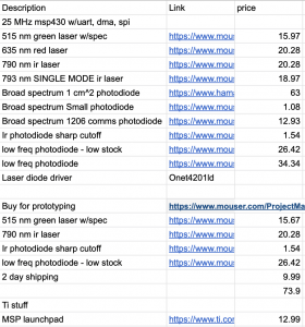
I spent this week designing our pcb and selecting every active component. This took a very long time because our application is very niche, so few parts exist that meet all of our requirements, and we need to have all the pieces fit together. This led to changing the design many times and reading datasheets for practically every part available for the some components, like laser diodes, photodiodes, and transimpedance amplifiers. This resulted in a now complete architecture and component selection that just needs to be filled in with passive component values to create a complete schematic. We do not expect to need to purchase passive components, as we have access to them from labs.
I worked with Anju and Roger to design our communication protocol. They were in charge of this, but I expressed some opinions and made sure their design is compatible with my PCB design.
I also worked with Anju and Roger to pick which FTDI chip to use for USB, since they have software requirements as well as the hardware requirements of the subsystem. After switching between many options, we finally settled on one.
I completed a budget for us. I ordered laser lenses for testing and factored in pcb fabrication and 3d printing cost to find how much our current plan will cost. We will have about $50 of buffer to handle anything we need to buy later on. This could go up with more selective buying extra parts than just buying 4 BOMs.
I tested the green laser diode to verify it works exactly as expected, and it does. I also tested the other components we bought early for testing, and found that none of them do what we want. This is very valuable because through this, I have learned how the optical components work and how they must be used in designs, so our final design will be well informed.
Schedule
My work is on schedule. I wanted to test parts this week, which I was able to do last week. This week, I got ahead on creating a complete design of the PCB and selected every part, which should make me continue to be a bit ahead next week, when I am expecting to create a complete schematic. While I do not have the schematic yet, I have a complete enough design that the schematic will be pretty quick.
Deliverables
I hope to complete our schematic for our pcb in the next week. I also hope to test our newly purchased lenses with Anju when they arrive to make sure we will be able to use them.
Principles Used This Week
Circuits:
I used principles from 18220: Electronic Devices and Analog Circuits for designing our circuits. However, most of the knowledge I have about circuits comes from my work outside regular classes working on Moonranger, a lunar rover research project (16861: Space Robotics, 16865: Space Robotics Development, 16597: Robotics Reading and Research). I also have learned principles of analog design from prior internships.
Protocol Design:
I used some principles from 18240: Structure and Design of Digital Systems and 18349: Introduction to Embedded Systems to help with designing the protocol this week, as I used FPGA knowledge and knowledge of existing protocols used in embedded systems. My knowledge that helped with this also comes primarily from research outside class as well, as I have written a lot of embedded code for research and for internships.
Optics:
I have no familiarity with optics and optical circuits. I learned about optical circuits, how they work, and common designs through a lot of online research reading datasheets, reference designs, and guides on creating various optical circuits and communication systems. I mostly learned from fiber optic and time-of-flight laser system designs.
FPGA chips were difficult to find, so we plan to switch to using a separate FPGA dev board or a microcontroller
Dev board may have latency issues because high-speed communication will need to be sent back and forth over wires to a separate PCB
Microcontroller speed/data transmission also has a latency issue, because it’s slower than FPGA
MCU speed: with the MSP430 that we’ve used before, 25MHz is the fastest option.
We could also use 2 microcontrollers to mitigate the speed issue, and use 1 per laser
Plan: test out both the microcontroller and FPGA dev board in a separate setting to choose which option
Component availability between early stage of design and component ordering
Some components are low stock. We will order components once we are confident we will be using rather than ordering once our pcb design is released
Lasers may not meet speed requirements
If not all components that we selected work, we will swap to a single laser setup using the one that works. We are confident that green will work because it has specs for modulation frequency, but the IR laser does not. We plan on testing this next week.
Design Changes
Change to FPGA
As described above, we were unable to find a FPGA to put on our custom PCB, so we will need to either use a FPGA dev board or MSP430 microcontroller.
Not using sinusoidal modulation
We will instead send a square signal over the laser. This is because fiber optic laser drivers do this as well, so there is no commercially available IC to modulate a sinusoid with enough current to power our laser.
Not use fiber optic laser driver
After creating a partial schematic and selecting support components for fiber optic drivers, it became clear that our application has a large number of changes required to manufacturer suggestions in order to work. Our project will be easier and more likely to succeed if we just create the driver circuits discretely rather than using a modified fiber optic driver circuit.
Switch to 2 lasers: IR and green
We found that blue lasers are very expensive and there is only one with a low enough power rating for us, and it is most likely too slow. As a result, we switched to 2 lasers. Changing red to IR makes the gap in wavelength larger, so we can use commercially available photodiodes that only receive light at certain wavelengths to filter out the other color.
Considering adding a higher voltage power supply
The green laser has a forward voltage over 5V. We are concerned about the effect that a boost converter will have on signal integrity, and do not consider our power supply to be the important part of our system.
Our project includes considerations for safety and security
Safety: The lasers must be of low enough power to not injure the eyes of users and bystanders
Security: Our use case concerns itself with the secure transfer of private information. This method should ensure the private and secure transmission of data with minimal chance for remote interception.
Schedule Changes
Because we are unsure if we’re using FPGA now, Anju will test out and set up environments for microcontrollers and FPGA to test out the parts for next week.
I worked with Anju on picking an FPGA and finding a development board to get her started on writing Verilog before the final PCB is designed and assembled. I looked at some microcontrollers as potential options since she could not find an fpga for us to put on a custom board, and worked with her to determine how to test if using an FPGA dev board will be fast enough.
I specced and ordered lasers and photodiodes to evaluate their performance with high frequency modulation to make sure they are fast enough for our needs. We are ordering a green laser and blue photodiode, and an IR laser and photodiode. The photodiodes have poor performance at the wavelengths of the other laser, since green and IR are far apart. This way, we do not need to do any filtering ourselves to pick out each color laser.
I began considering fiber optic laser drivers for use for driving our free space lasers. They do not meet our design requirements, so I began making a schematic to see if one could still be used with modification to manufacturer recommended support circuitry. It ended up having a lot of potential problems, so we probably will not go this route, and will use discrete circuits to drive the laser. Between doing calculations for component values on my own and TI’s responses to my questions about their drivers, it seems that it might not work once we have the final boards in hand, which is too big a risk for us to take.
I began designing a circuit to drive the laser with discrete components. This is probably what we will end up using.
Schedule
My work is on schedule. I wanted to buy the lasers and photodiodes this week to test their performance at high frequency, which I did. I got a bit further into schematic work this week than I expected as well.
The lack of FPGA chips available means that we have not selected a processor yet, which could put us behind schedule soon. Our fallback plan is to use an MSP430, because Anju and I are familiar with the software and I am familiar with hardware and confident I can make a board with one quickly.
Deliverables
In the next week, I hope to have a complete schematic of the transmitter, and an idea of some part selection for the receiver. I also hope to have come to a decision with Anju about what our processor will be, and a plan with Roger about how to verify that the board will work at our speed.