- Work this week
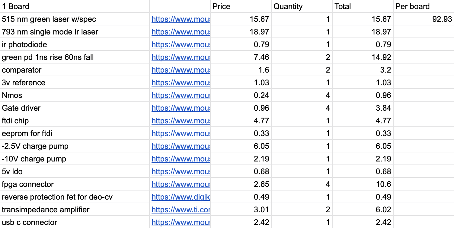
- I spent this week designing our pcb and selecting every active component. This took a very long time because our application is very niche, so few parts exist that meet all of our requirements, and we need to have all the pieces fit together. This led to changing the design many times and reading datasheets for practically every part available for the some components, like laser diodes, photodiodes, and transimpedance amplifiers. This resulted in a now complete architecture and component selection that just needs to be filled in with passive component values to create a complete schematic. We do not expect to need to purchase passive components, as we have access to them from labs.
- I worked with Anju and Roger to design our communication protocol. They were in charge of this, but I expressed some opinions and made sure their design is compatible with my PCB design.
- I also worked with Anju and Roger to pick which FTDI chip to use for USB, since they have software requirements as well as the hardware requirements of the subsystem. After switching between many options, we finally settled on one.
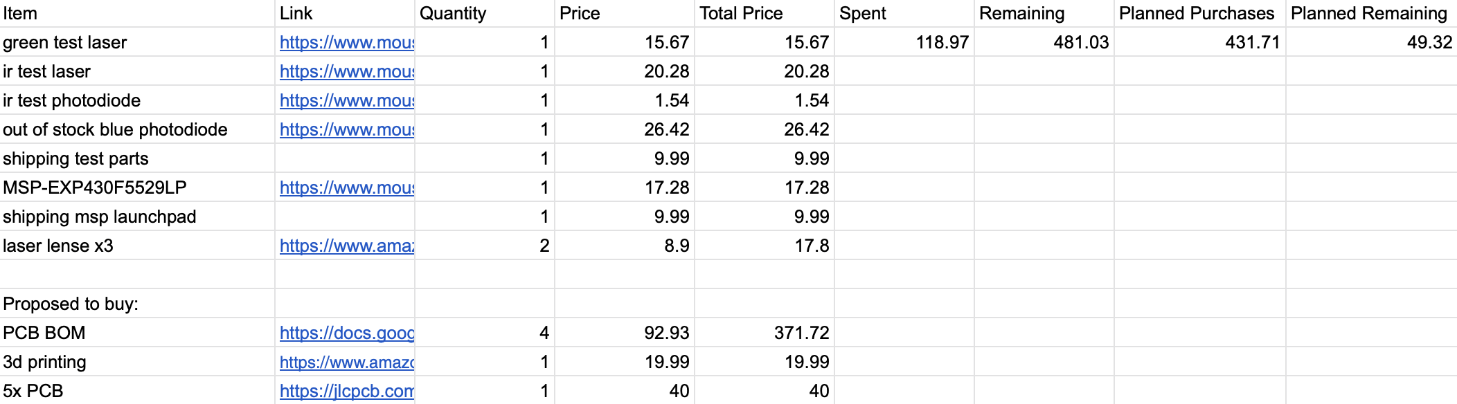
- I completed a budget for us. I ordered laser lenses for testing and factored in pcb fabrication and 3d printing cost to find how much our current plan will cost. We will have about $50 of buffer to handle anything we need to buy later on. This could go up with more selective buying extra parts than just buying 4 BOMs.
- I tested the green laser diode to verify it works exactly as expected, and it does. I also tested the other components we bought early for testing, and found that none of them do what we want. This is very valuable because through this, I have learned how the optical components work and how they must be used in designs, so our final design will be well informed.
- I spent this week designing our pcb and selecting every active component. This took a very long time because our application is very niche, so few parts exist that meet all of our requirements, and we need to have all the pieces fit together. This led to changing the design many times and reading datasheets for practically every part available for the some components, like laser diodes, photodiodes, and transimpedance amplifiers. This resulted in a now complete architecture and component selection that just needs to be filled in with passive component values to create a complete schematic. We do not expect to need to purchase passive components, as we have access to them from labs.
- Schedule
- My work is on schedule. I wanted to test parts this week, which I was able to do last week. This week, I got ahead on creating a complete design of the PCB and selected every part, which should make me continue to be a bit ahead next week, when I am expecting to create a complete schematic. While I do not have the schematic yet, I have a complete enough design that the schematic will be pretty quick.
- Deliverables
- I hope to complete our schematic for our pcb in the next week. I also hope to test our newly purchased lenses with Anju when they arrive to make sure we will be able to use them.
- Principles Used This Week
- Circuits:
- I used principles from 18220: Electronic Devices and Analog Circuits for designing our circuits. However, most of the knowledge I have about circuits comes from my work outside regular classes working on Moonranger, a lunar rover research project (16861: Space Robotics, 16865: Space Robotics Development, 16597: Robotics Reading and Research). I also have learned principles of analog design from prior internships.
- Protocol Design:
- I used some principles from 18240: Structure and Design of Digital Systems and 18349: Introduction to Embedded Systems to help with designing the protocol this week, as I used FPGA knowledge and knowledge of existing protocols used in embedded systems. My knowledge that helped with this also comes primarily from research outside class as well, as I have written a lot of embedded code for research and for internships.
- Optics:
- I have no familiarity with optics and optical circuits. I learned about optical circuits, how they work, and common designs through a lot of online research reading datasheets, reference designs, and guides on creating various optical circuits and communication systems. I mostly learned from fiber optic and time-of-flight laser system designs.
- Circuits:
Anju Ito, Roger Lacson, and KJ Newman