
Progress
Audio
I wrote a SystemVerilog testbench to test loading note data from a file and converting it to a waveform. The note data is stored in a simple hex format: all notes are on an eighth-note grid, and each note is a value from 1 to 108 (0x6C). 1 represents C0 and 108 represents B8. The music module uses several counters to time waveform generation (calculated at 50MHz), the 50kHz audio sampling rate, and the eighth-note tempo of the song (4 Hz at 120 bpm).
I first wrote a simple Python script to translate human-readable note values into hex note values, like so:
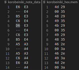
The left column is the lead voice, and the right column is the bass accompaniment. “00” is used to encode an eighth-note rest.
There are three modules that work together to turn this .mem file into music:
-
note_freq_lookup
-
wavegen
-
music
As each note value is read from the music file, the note_freq_lookup module translates it from a note number to a wavelength, expressed in terms of 50MHz cycles. Then the wavegen module calculates the value of the signal based on the wavelength and a 50MHz clock counter. The music module samples the output of the wave generator at 50kHz, generating the final audio signal.
The next step with the audio is to run some hardware tests. I plan to write a simpler test of the DAC hardware first, and then integrate the music module with the DAC testbench to test full audio output.
Controllers
We initially planned to only fabricate one PCB, which would basically be a breakout board for our buttons. We’d have a generic 2×6 pin connector that could connect to the GPIO pins on the FPGA, and pads to solder button leads to. The DAC and audio jack would be on a breadboard or a piece of protoboard. The problem with this design is that we’d have to have multiple cables plugged into the GPIO 2×20 header. There would be three: one for the controller, one for the audio, and one for networking. We didn’t like the idea of splicing and soldering a custom 3-to-1 cable, since the wires in the ribbon cables are so small and delicate. And trying to plug three separate connectors into one header wouldn’t work either, since the connector’s housings are too big to fit into the GPIO header side-by-side. Our first solution was to create a “middleman” board that would accept a 2×20 ribbon cable from each FPGA, and have each of the pins routed to the proper corresponding pin on a smaller connector. Our second solution was to break the middleman board into two symmetric boards, so that each FPGA could have its own board that would connect to its own controller and audio unit. This way we can package an middleman board with each FPGA to make two self-contained “consoles” that can network directly, rather than having an extra piece of hardware to connect the two. Another pro is that this would allow us to move the audio hardware onto this board as well.
This week was primarily spent sourcing components for this board and figuring out the design for the middleman board. This included picking which connectors to use and deciding on a pinout for each connector. I assigned the pins for the networking based on Eric’s TSPIN protocol, picked the pins for the controller connector such that the button layout can be flipped for left-handed players by inverting the connector, and laid out everything else based on what would be easiest to route. I also had a few extra pins on each connector, which I decided to connect to unused GPIO pins in case we end up needing them later (NX[0..3] and CX[0..3]). I ended up with this:
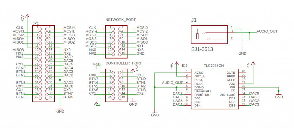
The next thing to do for the middleman board is also to test the DAC. Once I can verify the wiring is correct, it will be ready for fabrication. I checked the cost of the board on OSH Park and it’ll be $18.45 for 3 boards, which is well within our budget. We’ll get some extras to be safe.
Schedule
I’m a little ahead of schedule with the music module, and right on schedule with controllers. This next week I plan to test the DAC in hardware and send out the controller PCB and the middleman PCB for fabrication. I also want to do some experiments with hardware debouncing for the controller buttons using an low-pass filter RC circuit. I’ll also start designing the enclosure for the controller as well as possibly one for the middleman board.